SLLS629L January 2006 – October 2015 ISO721 , ISO721M , ISO722 , ISO722M
PRODUCTION DATA.
- 1 Features
- 2 Applications
- 3 Description
- 4 Revision History
- 5 Device Comparison Table
- 6 Pin Configuration and Functions
-
7 Specifications
- 7.1 Absolute Maximum Ratings
- 7.2 ESD Ratings
- 7.3 Recommended Operating Conditions
- 7.4 Thermal Information
- 7.5 Electrical Characteristics, 5 V
- 7.6 Electrical Characteristics, 5 V, 3.3 V
- 7.7 Electrical Characteristics, 3.3 V, 5 V
- 7.8 Electrical Characteristics, 3.3 V
- 7.9 Power Dissipation
- 7.10 Switching Characteristics, 5 V
- 7.11 Switching Characteristics, 5 V, 3.3 V
- 7.12 Switching Characteristics, 3.3 V, 5 V
- 7.13 Switching Characteristics, 3.3 V
- 7.14 Typical Characteristics
- 8 Parameter Measurement Information
- 9 Detailed Description
- 10Application and Implementation
- 11Power Supply Recommendations
- 12Layout
- 13Device and Documentation Support
- 14Mechanical, Packaging, and Orderable Information
Package Options
Mechanical Data (Package|Pins)
- D|8
Thermal pad, mechanical data (Package|Pins)
Orderable Information
12 Layout
12.1 Layout Guidelines
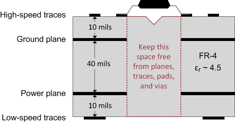
A minimum of four layers is required to accomplish a low EMI PCB design as shown in Figure 23. Layer stacking should be in the following order (top-to-bottom): high-speed signal layer, ground plane, power plane, and low-frequency signal layer.
- Routing the high-speed traces on the top layer avoids the use of vias (and the introduction of their inductances) and allows for clean interconnects between the isolator and the transmitter and receiver circuits of the data link.
- Placing a solid ground plane next to the high-speed signal layer establishes controlled impedance for transmission line interconnects and provides an excellent low-inductance path for the return current flow.
- Placing the power plane next to the ground plane creates additional high-frequency bypass capacitance of approximately 100 pF/in2.
- Routing the slower speed control signals on the bottom layer allows for greater flexibility as these signal links usually have margin to tolerate discontinuities such as vias.
12.1.1 PCB Material
For digital circuit boards operating below 150 Mbps, (or rise and fall times higher than 1 ns), and trace lengths of up to 10 inches, use standard FR-4 epoxy-glass as PCB material. FR-4 (Flame Retardant 4) meets the requirements of Underwriters Laboratories UL94-V0, and is preferred over cheaper alternatives due to its lower dielectric losses at high frequencies, less moisture absorption, greater strength and stiffness, and its self- extinguishing flammability-characteristics.
12.2 Layout Example
 Figure 23. Recommended Layer Stack