SLLSEA5C March 2012 – March 2019 ISO7421E-Q1
PRODUCTION DATA.
- 1 Features
- 2 Applications
- 3 Description
- 4 Pin Configuration and Functions
- 5 Electrostatic Discharge Caution
- 6 Absolute Maximum Ratings
- 7 Thermal Information
- 8 Recommended Operating Conditions
- 9 Electrical Characteristics
- 10Switching Characteristics
- 11Electrical Characteristics
- 12Switching Characteristics
- 13Electrical Characteristics
- 14Switching Characteristics
- 15Electrical Characteristics
- 16Switching Characteristics
- 17Parameter Measurement Information
- 18Device Information
- 19Typical Characteristics
- 20Revision History
Package Options
Mechanical Data (Package|Pins)
- DW|16
Thermal pad, mechanical data (Package|Pins)
- DW|16
Orderable Information
18.5 IEC Safety Limiting Values
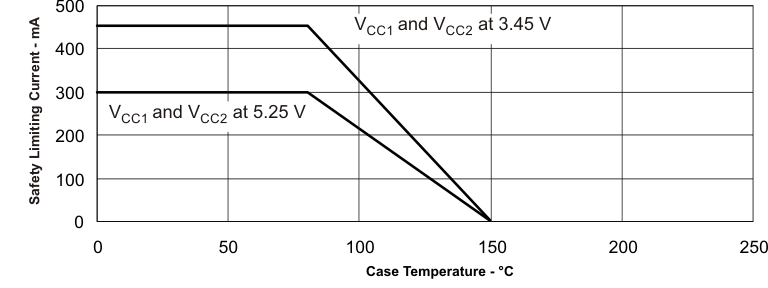
Safety limiting intends to prevent potential damage to the isolation barrier upon failure of input or output circuitry. A failure of the IO can allow low resistance to ground or the supply and, without current limiting, dissipate sufficient power to overheat the die and damage the isolation barrier potentially leading to secondary system failures.
| PARAMETER | TEST CONDITIONS | MIN | TYP | MAX | UNIT | |
|---|---|---|---|---|---|---|
| Is | Safety input, output, or supply current | θJA =212°C/W, VI = 5.5 V, TJ = 170°C, TA = 25°C | 112 | mA | ||
| θJA =212°C/W, VI = 3.6 V, TJ = 170°C, TA = 25°C | 171 | |||||
| Ts | Maximum Case Temperature | 150 | °C | |||
The safety-limiting constraint is the absolute maximum junction temperature specified in the absolute maximum ratings table. The power dissipation and junction-to-air thermal impedance of the device installed in the application hardware determines the junction temperature. The assumed junction-to-air thermal resistance in the Thermal Characteristics table is that of a device installed on a High-K Test Board for Leaded Surface Mount Packages. The power is the recommended maximum input voltage times the current. The junction temperature is then the ambient temperature plus the power times the junction-to-air thermal resistance.
 Figure 4. DW-16 Theta-JC Thermal Derating Curve per IEC 60747-5-2
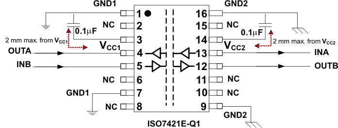
  Figure 5. Typical ISO7421E-Q1 Application Circuit