SLLSER1H August 2017 – January 2024 ISO7760 , ISO7761 , ISO7762 , ISO7763
PRODUCTION DATA
- 1
- 1 Features
- 2 Applications
- 3 Description
- 4 Pin Configuration and Functions
-
5 Specifications
- 5.1 Absolute Maximum Ratings
- 5.2 ESD Ratings
- 5.3 Recommended Operating Conditions
- 5.4 Thermal Information
- 5.5 Power Ratings
- 5.6 Insulation Specifications
- 5.7 Safety-Related Certifications
- 5.8 Safety Limiting Values
- 5.9 Electrical Characteristics—5-V Supply
- 5.10 Supply Current Characteristics—5-V Supply
- 5.11 Electrical Characteristics—3.3-V Supply
- 5.12 Supply Current Characteristics—3.3-V Supply
- 5.13 Electrical Characteristics—2.5-V Supply
- 5.14 Supply Current Characteristics—2.5-V Supply
- 5.15 Switching Characteristics—5-V Supply
- 5.16 Switching Characteristics—3.3-V Supply
- 5.17 Switching Characteristics—2.5-V Supply
- 5.18 Insulation Characteristics Curves
- 5.19 Typical Characteristics
- 6 Parameter Measurement Information
- 7 Detailed Description
- 8 Application and Implementation
- 9 Power Supply Recommendations
- 10Layout
- 11Device and Documentation Support
- 12Revision History
- 13Mechanical, Packaging, and Orderable Information
Package Options
Mechanical Data (Package|Pins)
Thermal pad, mechanical data (Package|Pins)
- DW|16
Orderable Information
8.2.3.1 Insulation Lifetime
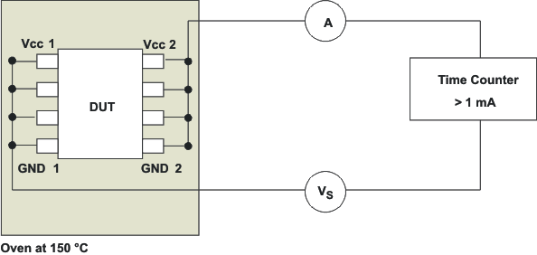
Insulation lifetime projection data is collected by using industry-standard Time Dependent Dielectric Breakdown (TDDB) test method. In this test, all pins on each side of the barrier are tied together creating a two-terminal device and high voltage applied between the two sides; See Figure 8-6for TDDB test setup. The insulation breakdown data is collected at various high voltages switching at 60 Hz over temperature. For reinforced insulation, VDE standard requires the use of TDDB projection line with failure rate of less than 1 part per million (ppm). Even though the expected minimum insulation lifetime is 20 years at the specified working isolation voltage, VDE reinforced certification requires additional safety margin of 20% for working voltage and 50% for lifetime which translates into minimum required insulation lifetime of 30 years at a working voltage that's 20% higher than the specified value.
Figure 8-7 shows the intrinsic capability of the isolation barrier to withstand high voltage stress over its lifetime. Based on the TDDB data, the intrinsic capability of the insulation is 1500 VRMS with a lifetime of 36 years. Other factors, such as package size, pollution degree, material group, etc. can further limit the working voltage of the component. The working voltage of DW-16 package is specified upto 1500 VRMS and DBQ-16 package up to 400 VRMS. At the lower working voltages, the corresponding insulation lifetime is much longer than 36 years.
 Figure 8-6 Test Setup for Insulation Lifetime Measurement
 Figure 8-7 Insulation Lifetime Projection
Data