SLLSFF7A may 2021 – december 2021 ISOW1044
PRODUCTION DATA
- 1
- 1 Features
- 2 Applications
- 3 Description
- 4 Revision History
- 5 Description Continued
- 6 Device Comparison Table
- 7 Pin Configuration and Functions
-
8 Specifications
- 8.1 Absolute Maximum Ratings
- 8.2 ESD Ratings
- 8.3 Recommended Operating Conditions
- 8.4 ThermalInformation
- 8.5 Power Ratings
- 8.6 Insulation Specifications
- 8.7 Safety-Related Certifications
- 8.8 Safety Limiting Values
- 8.9 Electrical Characteristics
- 8.10 Supply Current Characteristics
- 8.11 Switching Characteristics
- 8.12 Insulation Characteristics Curves
- 8.13 Typical Characteristics
- 9 Parameter Measurement Information
- 10Detailed Description
- 11Application and Implementation
- 12Power Supply Recommendations
- 13Layout
- 14Device and Documentation Support
- 15Mechanical, Packaging, and Orderable Information
Package Options
Mechanical Data (Package|Pins)
- DFM|20
Thermal pad, mechanical data (Package|Pins)
Orderable Information
9 Parameter Measurement Information
 Figure 9-1 Driver Voltage,
Current and Test Definitions
Figure 9-1 Driver Voltage,
Current and Test Definitions Figure 9-2 Bus Logic State
Voltage Definitions
Figure 9-2 Bus Logic State
Voltage Definitions
Figure 9-3 Driver Test Circuit and Voltage
Waveforms. 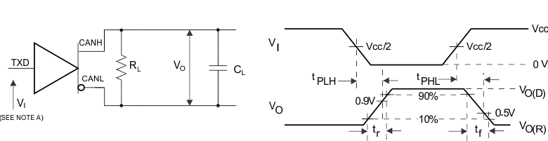
A.
The input pulse is supplied by a generator having the following characteristics: PRR ≤ 125 kHz, 50% duty cycle, tr ≤ 6 ns, tf ≤ 6 ns, ZO = 50 Ω.
 Figure 9-4 Receiver Voltage
and Current Definitions
Figure 9-4 Receiver Voltage
and Current Definitions
A. The input pulse is supplied by a generator
having the following characteristics: PRR ≤ 125 kHz, 50% duty cycle,
tr ≤ 6 ns, tf ≤ 6 ns, ZO = 50 Ω.
Figure 9-5 Receiver Test
Circuit and Voltage Waveformstr ≤ 6 ns, tf ≤ 6 ns, ZO = 50 Ω.
Table 9-1 Receiver Differential Input Voltage
Threshold Test
| INPUT | OUTPUT | |||
|---|---|---|---|---|
| VCANH | VCANL | |VID| | RXD | |
| -11.5 V | -12.5 V | 1000 mV | L | VOL |
| 12.5 V | 11.5 V | 1000 mV | L | |
| -8.55 V | -9.45 V | 900 mV | L | |
| 9.45 V | 8.55 V | 900 mV | L | |
| -8.75 V | -9.25 V | 500 mV | H | VOH |
| 9.25 V | 8.75 V | 500 mV | H | |
| -11.8 V | -12.2 V | 400 mV | H | |
| 12.2 V | 11.8 V | 400 mV | H | |
| Open | Open | X | H | |
 Figure 9-6 tLOOP
and CAN FD Timing Parameter Measurement
Figure 9-6 tLOOP
and CAN FD Timing Parameter Measurement
A. The input pulse is supplied by a
generator having the following characteristics: tr ≤ 6 ns, tf ≤ 6
ns, ZO = 50 Ω.
Figure 9-7 Dominant Time-out
Test Circuit and Voltage Waveforms Figure 9-8 Driver
Short-Circuit Current Test Circuit and Waveforms
Figure 9-8 Driver
Short-Circuit Current Test Circuit and Waveforms Figure 9-9 Common-Mode
Transient Immunity Test Circuit
Figure 9-9 Common-Mode
Transient Immunity Test Circuit
A. VCCI and VCCO
refers to the power supplies VIO and VISOIN, respectively.
CL = 15 pF and The input pulse is supplied by a generator having the
following characteristics: PRR ≤ 50 kHz, 50% duty cycle, tr ≤ 3 ns,
tf ≤ 3ns, ZO = 50 Ω. At the input, 50 Ω resistor is required to
terminate Input Generator signal. It is not needed in actual application.
B. B. CL = 15 pF and includes
instrumentation and fixture capacitance within ±20%.
Figure 9-10 Switching
Characteristics Test Circuit and Voltage Waveforms