SNVSBF4 November 2019 LDC1001-Q1
PRODUCTION DATA.
- 1 Features
- 2 Applications
- 3 Description
- 4 Revision History
- 5 Pin Configuration and Functions
- 6 Specifications
-
7 Detailed Description
- 7.1 Overview
- 7.2 Functional Block Diagram
- 7.3 Feature Description
- 7.4 Device Functional Modes
- 7.5 Programming
- 7.6
Register Map
- 7.6.1
Register Description
- 7.6.1.1 Revision ID (offset = 0x00) [reset = 0x80]
- 7.6.1.2 Rp_MAX (offset = 0x01) [reset = 0x0E]
- 7.6.1.3 Rp_MIN (offset = 0x02) [reset = 0x14]
- 7.6.1.4 Sensor Frequency (offset = 0x03) [reset = 0x45]
- 7.6.1.5 LDC Configuration (offset = 0x04) [reset = 0x1B]
- 7.6.1.6 Clock Configuration (offset = 0x05) [reset = 0x01]
- 7.6.1.7 Comparator Threshold High LSB (offset = 0x06) [reset = 0xFF]
- 7.6.1.8 Comparator Threshold High MSB (offset = 0x07) [reset = 0xFF]
- 7.6.1.9 Comparator Threshold Low LSB (offset = 0x08) [reset = 0x00]
- 7.6.1.10 Comparator Threshold Low MSB (offset = 0x09) [reset = 0x00]
- 7.6.1.11 INTB Pin Configuration (offset = 0x0A) [reset = 0x00]
- 7.6.1.12 Power Configuration (offset = 0x0B) [reset = 0x00]
- 7.6.1.13 Status (offset = 0x20) [reset = NA]
- 7.6.1.14 Proximity Data LSB (offset = 0x21) [reset = NA]
- 7.6.1.15 Proximity Data MSB (offset = 0x22) [reset = NA]
- 7.6.1.16 Frequency Counter LSB (offset = 0x23) [reset = NA]
- 7.6.1.17 Frequency Counter Mid-Byte (offset = 0x24) [reset = NA]
- 7.6.1.18 Frequency Counter MSB (offset = 0x25) [reset = NA]
- 7.6.1
Register Description
- 8 Application and Implementation
- 9 Power Supply Recommendations
- 10Layout
- 11Device and Documentation Support
- 12Mechanical, Packaging, and Orderable Information
Package Options
Mechanical Data (Package|Pins)
- PW|16
Thermal pad, mechanical data (Package|Pins)
Orderable Information
7.3.2 Measuring Parallel Resonance Impedance and Inductance With LDC1001-Q1
Remember that the LDC1001-Q1 can determine the value of RP by monitoring the amount of power injected into the resonator. The device returns this value as a digital value which is inversely proportional to RP. The LDC1001-Q1 device can also measure the oscillation frequency of the LC circuit, which can be used to determine the inductance of the LC circuit. The oscillation frequency is returned as a digital value.
The LDC1001-Q1 device supports a wide range of LC combinations with oscillation frequencies ranging from 5 kHz to 5 MHz and RP ranging from 798 Ω to 3.93 MΩ. This range of RP can be viewed as the maximum input range of an ADC. As shown in Figure 9, the range of RP is typically much smaller than maximum input range supported by the LDC1001-Q1 device. To achieve better resolution in the desired sensing range, the LDC1001-Q1 device offers a programmable input range through the Rp_MIN and Rp_MAX registers. See the Calculation of Rp_Min and Rp_Max section for how to set these registers.
When the resonance impedance of the sensor, RP, drops below the programed Rp_MIN, the RP output of the LDC will clip at the full scale output. An example occurrence of this situation is when a target comes too close to the coil.
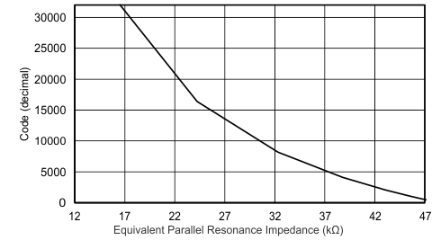
 Figure 10. Transfer Characteristics of LDC1001-Q1 With Rp_MIN = 16.160 kΩ and Rp_MAX = 48.481 kΩ
 Use Equation 3 to calculate the resonance impedance from the digital output code.
where
- Y = Proximity Data / 215
- Proximity data is the LDC output, register address 0x21 and 0x22.
Example: If Proximity data (address 0x22 to 0x21) is 5000, Rp_MIN is 2.394 kΩ, and Rp_MAX is 38.785 kΩ, the resonance impedance is given by:
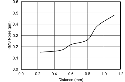
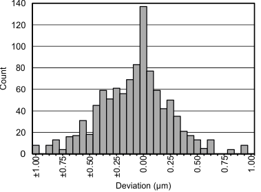
Figure 11 and Figure 12 show the change in RMS noise versus distance and a histogram of noise, with the target at an 0.8-mm distance from the sensor coil. Data was collected with a 14-mm PCB coil (23 turns, 4-mil trace width, 4-mil spacing between trace, 1-oz copper thickness, FR4) with a sensing range of 0.125 mm to 1.125 mm. At a distance of 0.8 mm, the RMS noise is approximately 250 nm.
 Figure 11. Typical RMS Noise vs Distance With PCB Coil
  Figure 12. Histogram of Output Codes at 0.8-mm Distance
 NOTE
Although the LDC1001-Q1 device has high resolution, the absolute accuracy depends on offset and gain correction which can be achieved by two-point calibration.