SNVSBF7 November 2019 LDC1001
PRODUCTION DATA.
- 1 Features
- 2 Applications
- 3 Description
- 4 Revision History
- 5 Pin Configuration and Functions
- 6 Specifications
-
7 Detailed Description
- 7.1 Overview
- 7.2 Functional Block Diagram
- 7.3 Feature Description
- 7.4 Device Functional Modes
- 7.5 Programming
- 7.6
Register Maps
- 7.6.1
Register Description
- 7.6.1.1 Revision ID (Address = 0x00)
- 7.6.1.2 RP_MAX (Address = 0x01)
- 7.6.1.3 RP_MIN (Address = 0x02)
- 7.6.1.4 Watchdog Timer Frequency (Address = 0x03)
- 7.6.1.5 LDC Configuration (Address = 0x04)
- 7.6.1.6 Clock Configuration (Address = 0x05)
- 7.6.1.7 Comparator Threshold High LSB (Address = 0x06)
- 7.6.1.8 Comparator Threshold High MSB (Address = 0x07)
- 7.6.1.9 Comparator Threshold Low LSB (Address = 0x08)
- 7.6.1.10 Comparator Threshold Low MSB (Address = 0x09)
- 7.6.1.11 INTB Pin Configuration (Address = 0x0A)
- 7.6.1.12 Power Configuration (Address = 0x0B)
- 7.6.1.13 Status (Address = 0x20)
- 7.6.1.14 Proximity Data LSB (Address = 0x21)
- 7.6.1.15 Proximity Data MSB (Address = 0x22)
- 7.6.1.16 Frequency Counter LSB (Address = 0x23)
- 7.6.1.17 Frequency Counter Mid-Byte (Address = 0x24)
- 7.6.1.18 Frequency Counter MSB (Address = 0x25)
- 7.6.1
Register Description
- 8 Application and Implementation
- 9 Power Supply Recommendations
- 10Layout
- 11Device and Documentation Support
- 12Mechanical, Packaging, and Orderable Information
Package Options
Mechanical Data (Package|Pins)
- NHR|16
Thermal pad, mechanical data (Package|Pins)
Orderable Information
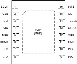
5 Pin Configuration and Functions
NHR Package
16-Pin WSON
Top View

Pin Functions
| PIN | TYPE(1) | DESCRIPTION | |
|---|---|---|---|
| NO. | NAME | ||
| 1 | SCLK | DI | SPI clock input. SCLK is used to clock-out/clock-in the data from/into the chip. |
| 2 | CSB | DI | SPI CSB. Multiple devices can be connected on the same SPI bus with each device having a dedicated CSB connection to the MCU so that each device can be uniquely selected. |
| 3 | SDI | DI | SPI Slave Data In (Master Out Slave In). This should be connected to the Master Out Slave In of the master. |
| 4 | VIO | P | Digital IO Supply |
| 6 | DGND | P | Digital ground |
| 5 | SDO | DO | SPI Slave Data Out (Master In Slave Out). This pin is high-Z when CSB is high. |
| 7 | CFB | A | LDC filter capacitor |
| 8 | CFA | A | LDC filter capacitor |
| 9 | INA | A | External LC Tank. Connected to external LC tank |
| 10 | INB | A | External LC Tank. Connected to external LC tank |
| 11 | GND | P | Analog ground |
| 12 | VDD | P | Analog supply |
| 13 | CLDO | A | LDO bypass capacitor. A 56-nF capacitor should be connected from this pin to GND. |
| 14 | TBCLK | DI/A | External time-base clock |
| 15 | NC | NC | This pin should be left floating. |
| 16 | INTB | DO | Configurable interrupt output. |
| — | DAP | P | Connect to GND for improved thermal performance.(2) |
(1) DO: Digital Output, DI: Digital Input, P: Power, A: Analog
(2) There is an internal electrical connection between the exposed Die Attach Pad (DAP) and the GND pin of the device. Although the DAP can be left floating, for best performance the DAP should be connected to the same potential as the devices's GND pin. Do no use the DAP as the primary ground for the device. The device GND pin must always be connected to ground.