SNOSDC7B December 2021 – December 2021 LDC3114-Q1
PRODUCTION DATA
- 1 Features
- 2 Applications
- 3 Description
- 4 Revision History
- 5 Pin Configuration and Functions
- 6 Specifications
-
7 Detailed Description
- 7.1 Overview
- 7.2 Functional Block Diagram
- 7.3 Feature Description
- 7.4 Device Functional Modes
- 7.5 Register Maps
-
8 Application and Implementation
- 8.1
Application Information
- 8.1.1 Theory of Operation
- 8.1.2 Designing Sensor Parameters
- 8.1.3 Setting COM Pin Capacitor
- 8.1.4 Defining Power-On Timing
- 8.1.5 Configuring Button or Raw Data Scan Rate
- 8.1.6 Programming Button or Raw Data Sampling Window
- 8.1.7 Scaling Frequency Counter Output
- 8.1.8 Setting Button Triggering Threshold
- 8.1.9 Tracking Baseline
- 8.1.10 Mitigating False Button Detections
- 8.1.11 Reporting Interrupts for Button Presses, Raw Data Ready and Error Conditions
- 8.1.12 Estimating Supply Current
- 8.2 Typical Application
- 8.1
Application Information
- 9 Power Supply Recommendations
- 10Layout
- 11Device and Documentation Support
- 12Mechanical, Packaging, and Orderable Information
Package Options
Mechanical Data (Package|Pins)
- PW|16
Thermal pad, mechanical data (Package|Pins)
Orderable Information
8.1.2 Designing Sensor Parameters
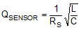
Figure 8-3 shows that each inductive touch button uses an LC resonator sensor, where L is the inductor, C is the capacitor, and RS is the AC series resistance of the sensor at the frequency of operation. The key parameters of the LC sensor include frequency, effective parallel resistance RP, and quality factor Q. These parameters must be within the ranges as specified in the Sensor section of the Section 6.5 table. Note that the effective RP and Q changes when the conductive target is in place.
 Figure 8-3 LC Resonator
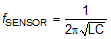
The LC sensor frequency defined in Equation 3 must be between 1 MHz and 30 MHz. For optimal performance, configure the sensor frequency to be greater than 3 MHz.
The sensor quality factor defined in Equation 4 must be between 5 and 30.
The series resistance defined in Equation 5 can be represented as an equivalent parallel resistance, RP.

 Figure 8-4 Equivalent Parallel Circuit
RP can be viewed as the load on the sensor driver. This load corresponds to the current drive required to maintain the oscillation amplitude. RP must be between 350 Ω and 10 kΩ.
In summary, the LDC3114-Q1 requires that the sensor parameters are within the following ranges when the conductive target is present:
- 1 MHz ≤ fSENSOR ≤ 30 MHz
- 5 ≤ Q ≤ 30
- 350 Ω ≤ RP ≤ 10 kΩ