SNOSDC7B December 2021 – December 2021 LDC3114-Q1
PRODUCTION DATA
- 1 Features
- 2 Applications
- 3 Description
- 4 Revision History
- 5 Pin Configuration and Functions
- 6 Specifications
-
7 Detailed Description
- 7.1 Overview
- 7.2 Functional Block Diagram
- 7.3 Feature Description
- 7.4 Device Functional Modes
- 7.5 Register Maps
-
8 Application and Implementation
- 8.1
Application Information
- 8.1.1 Theory of Operation
- 8.1.2 Designing Sensor Parameters
- 8.1.3 Setting COM Pin Capacitor
- 8.1.4 Defining Power-On Timing
- 8.1.5 Configuring Button or Raw Data Scan Rate
- 8.1.6 Programming Button or Raw Data Sampling Window
- 8.1.7 Scaling Frequency Counter Output
- 8.1.8 Setting Button Triggering Threshold
- 8.1.9 Tracking Baseline
- 8.1.10 Mitigating False Button Detections
- 8.1.11 Reporting Interrupts for Button Presses, Raw Data Ready and Error Conditions
- 8.1.12 Estimating Supply Current
- 8.2 Typical Application
- 8.1
Application Information
- 9 Power Supply Recommendations
- 10Layout
- 11Device and Documentation Support
- 12Mechanical, Packaging, and Orderable Information
Package Options
Mechanical Data (Package|Pins)
- PW|16
Thermal pad, mechanical data (Package|Pins)
Orderable Information
8.1.6 Programming Button or Raw Data Sampling Window
The sampling window is the actual duration per scan cycle for active data sampling of the sensor frequency. It is programmed with the exponential parameter, LCDIV, in Register LC_DIVIDER (Address 0x17), and the individual linear sensor cycle counter SENCYCn (n = 0, 1, 2, or 3) in Registers SENSORn_CONFIG (n = 0, 1, 2, or 3, Addresses 0x20, 0x22, 0x24, 0x26). For most touch button applications, the button sampling window should be set to between 1 ms and 8 ms. For sampling rate of 160 SPS, the window has to be less than 6.25 ms. For continuous sampling, the data becomes available at the configured sampling window period rate. The recommended minimum sensor conversion time is 1 ms. Longer conversion time can be used to achieve better signal-to-noise ratio, if needed. The active channels in Figure 8-6 will sample sequentially if multiple channels are enabled.
 Figure 8-6 Configurable Scan Rate
and Sampling Window
Figure 8-6 Configurable Scan Rate
and Sampling WindowThe LDC3114-Q1 is designed to work with LC resonator sensors with oscillation frequencies ranging from 1 MHz to 30 MHz. Equation 7 calculates the exact definition of the sampling window.
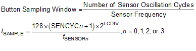
where:
- tSAMPLE is the sampling window in µs
- SENCYCn and LCDIV are the linear and exponential scalers that set the number of sensor oscillation cycles
- fSENSORn is the sensor frequency in MHz
In Equation 7, LCDIV (0 to 7, default 3) is the exponential LC divider that sets the approximate ranges for all channels, and SENCYCn (0 to 31, default 4) is the linear sensor cycle scaler that fine-tunes each individual channel. Together they set the number of sensor oscillation cycles used to determine the sampling window.
For example, if the LC sensor frequency is 9.2 MHz, and it is desirable to get 1-ms sampling window, then this can be achieved by setting SENCYCn = 17 and LCDIV = 2.
Alternatively, from the sampling window and sensor frequency, the LCDIV can be read off from Figure 8-7Figure 8-7. For example, 1-ms sampling window and 9.2-MHz sensor frequency intersect in the region closest to where LCDIV = 2. Then SENCYCn can be calculated accordingly.
 Figure 8-7 LCDIV as a Function of
Sensor Frequency and Button Sampling Window
Figure 8-7 LCDIV as a Function of
Sensor Frequency and Button Sampling Window