SNOSDD0 December 2021 LDC3114
PRODUCTION DATA
- 1 Features
- 2 Applications
- 3 Description
- 4 Revision History
- 5 Pin Configuration and Functions
- 6 Specifications
-
7 Detailed Description
- 7.1 Overview
- 7.2 Functional Block Diagram
- 7.3 Feature Description
- 7.4 Device Functional Modes
- 7.5 Register Maps
-
8 Application and Implementation
- 8.1
Application Information
- 8.1.1 Theory of Operation
- 8.1.2 Designing Sensor Parameters
- 8.1.3 Setting COM Pin Capacitor
- 8.1.4 Defining Power-On Timing
- 8.1.5 Configuring Button or Raw Data Scan Rate
- 8.1.6 Programming Button or Raw Data Sampling Window
- 8.1.7 Scaling Frequency Counter Output
- 8.1.8 Setting Button Triggering Threshold
- 8.1.9 Tracking Baseline
- 8.1.10 Mitigating False Button Detections
- 8.1.11 Reporting Interrupts for Button Presses, Raw Data Ready and Error Conditions
- 8.1.12 Estimating Supply Current
- 8.2 Typical Application
- 8.1
Application Information
- 9 Power Supply Recommendations
- 10Layout
- 11Device and Documentation Support
- 12Mechanical, Packaging, and Orderable Information
Package Options
Mechanical Data (Package|Pins)
- PW|16
Thermal pad, mechanical data (Package|Pins)
Orderable Information
5 Pin Configuration and Functions
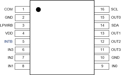
 Figure 5-1 LDC3114PW Package16-Pin TSSOPTop View
Table 5-1 Pin Functions
| PIN | I/O(1) | DESCRIPTION | |
|---|---|---|---|
| NAME | NO. | ||
| VDD | 4 | P | Power supply |
| GND | 2 | G | Ground(2) |
| 10 | |||
| INTB | 5 | O | Interrupt
output Polarity can be configured in Register 0x11. |
| LPWRB | 3 | I | Normal / Low
Power Mode select Set LPWRB to VDD for Normal Power Mode or ground for Low Power Mode. |
| COM | 1 | A | Common return
current path for all LC resonator sensors A capacitor should be connected from this pin to GND. Refer to Section 8.1.3. |
| IN0 | 9 | A | Channel 0 LC sensor input |
| IN1 | 8 | A | Channel 1 LC sensor input |
| IN2 | 7 | A | Channel 2 LC sensor input |
| IN3 | 6 | A | Channel 3 LC sensor input |
| OUT0 | 15 | O | Channel 0 logic
output Polarity can be configured in Register 0x1C. |
| OUT1 | 13 | O | Channel 1 logic
output Polarity can be configured in Register 0x1C. |
| OUT2 | 12 | O | Channel 2 logic
output Polarity can be configured in Register 0x1C. |
| OUT3 | 11 | O | Channel 3 logic
output Polarity can be configured in Register 0x1C. |
| SCL | 16 | I | I2C clock |
| SDA | 14 | I/O | I2C
data I2C address = 0x2A. |
(1) I = Input, O = Output, P=Power, G=Ground,
A=Analog
(2) Both pins should be connected to the
system ground on the PCB.