SNOS412Q February 2000 – January 2023 LM1117
PRODUCTION DATA
- 1 Features
- 2 Applications
- 3 Description
- 4 Revision History
- 5 Device Comparison Table
- 6 Pin Configuration and Functions
- 7 Specifications
- 8 Detailed Description
- 9 Application and Implementation
- 10Device and Documentation Support
- 11Mechanical, Packaging, and Orderable Information
Package Options
Mechanical Data (Package|Pins)
Thermal pad, mechanical data (Package|Pins)
- KTT|3
Orderable Information
8.3.1 Load Regulation
The LM1117 regulates the voltage that appears between the output and ground pins, or between the output and adjust pins. In some cases, line resistances can introduce errors to the voltage across the load. To obtain the best load regulation, a few precautions are needed.
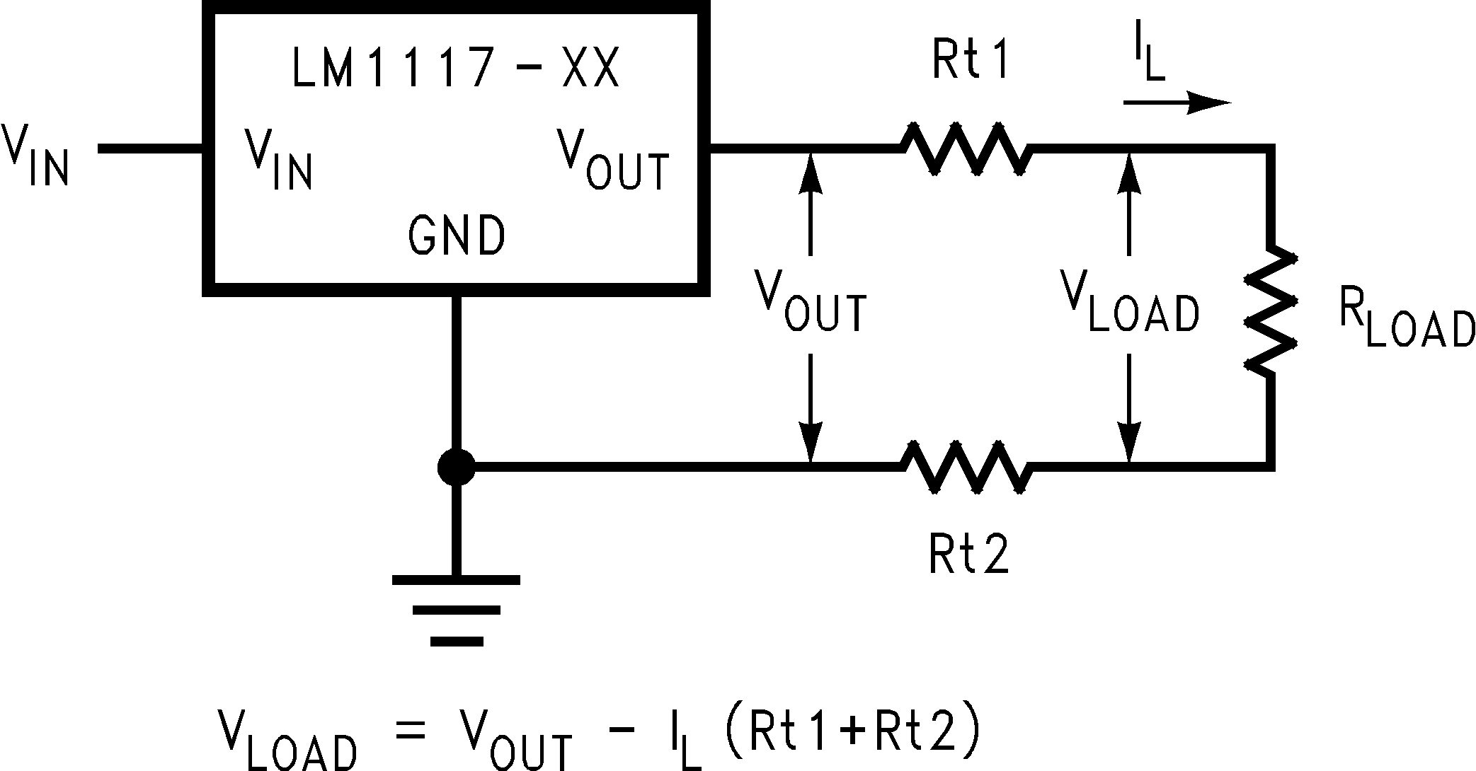
Figure 8-2 illustrates a typical application using a fixed output regulator. The Rt1 and Rt2 are the line resistances. Obviously the VLOAD is less than the VOUT by the sum of the voltage drops along the line resistances. In this case, the load regulation at the RLOAD is degraded from the data sheet specification. To improve this degradation, the load must be tied directly to the output terminal on the positive side and directly tied to the ground terminal on the negative side.
 Figure 8-2 Typical Application Using Fixed Output Regulator
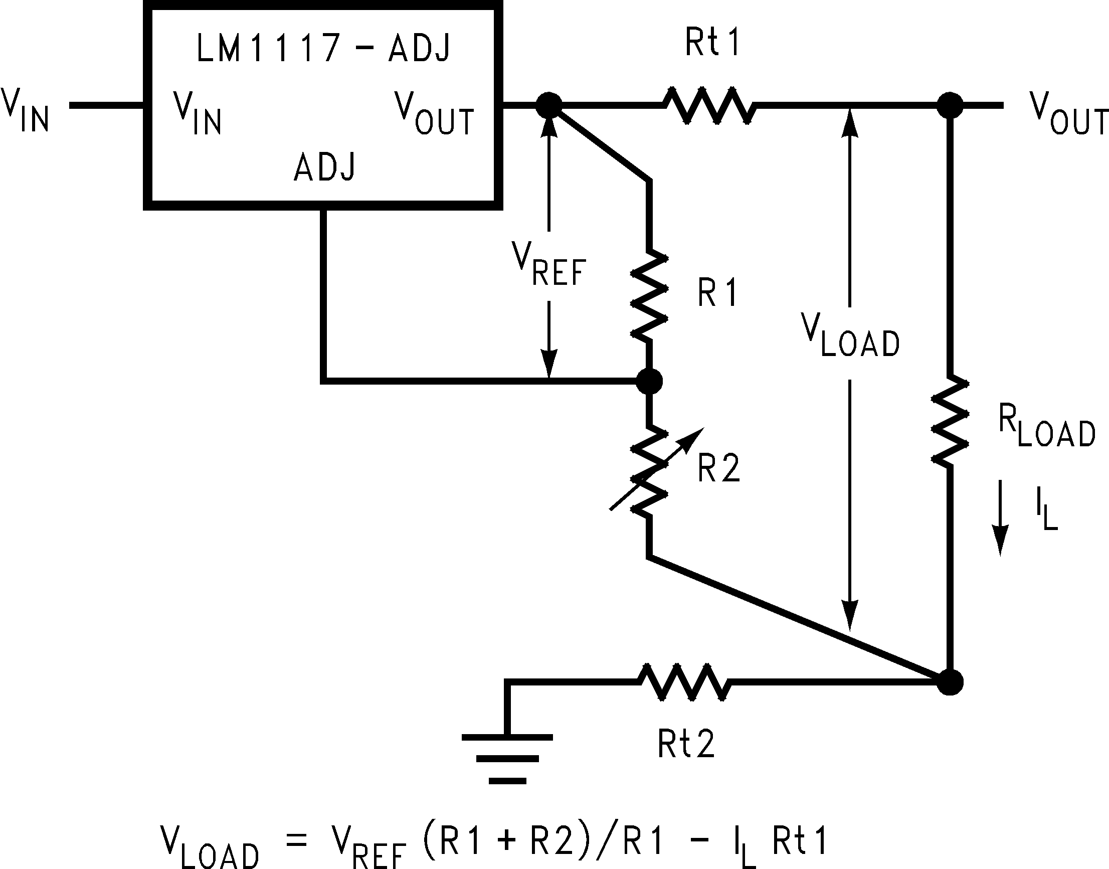
When the adjustable regulator is used (Figure 8-3), the best performance is obtained with the positive side of the resistor R1 tied directly to the output terminal of the regulator rather than near the load. This eliminates line drops from appearing effectively in series with the reference and degrading regulation. For example, a 5-V regulator with 0.05-Ω resistance between the regulator and load has a load regulation resulting from the line resistance of 0.05 Ω × IL. If R1 (= 125 Ω) is connected near the load, the effective line resistance is 0.05 Ω (1 + R2 / R1) or in this case, four times worse. In addition, the ground side of the resistor R2 can be returned near the ground of the load to provide remote ground sensing and improve load regulation.
 Figure 8-3 Best Load Regulation Using Adjustable Output Regulator