SNOS412Q February   2000  – January 2023 LM1117

PRODUCTION DATA  

  1. Features
  2. Applications
  3. Description
  4. Revision History
  5. Device Comparison Table
  6. Pin Configuration and Functions
  7. Specifications
    1. 7.1 Absolute Maximum Ratings
    2. 7.2 ESD Ratings
    3. 7.3 Recommended Operating Conditions
    4. 7.4 Thermal Information
    5. 7.5 LM1117 Electrical Characteristics
    6. 7.6 LM1117I Electrical Characteristics
    7. 7.7 Typical Characteristics
  8. Detailed Description
    1. 8.1 Overview
    2. 8.2 Functional Block Diagram
    3. 8.3 Feature Description
      1. 8.3.1 Load Regulation
    4. 8.4 Device Functional Modes
      1. 8.4.1 Protection Diodes
  9. Application and Implementation
    1. 9.1 Application Information
    2. 9.2 Typical Application
      1. 9.2.1 Design Requirements
      2. 9.2.2 Detailed Design Procedure
        1. 9.2.2.1 External Capacitors
          1. 9.2.2.1.1 Input Bypass Capacitor
          2. 9.2.2.1.2 Adjust Terminal Bypass Capacitor
          3. 9.2.2.1.3 Output Capacitor
      3. 9.2.3 Application Curve
    3. 9.3 System Examples
    4. 9.4 Power Supply Recommendations
    5. 9.5 Layout
      1. 9.5.1 Layout Guidelines
        1. 9.5.1.1 Heat Sink Requirements
      2. 9.5.2 Layout Example
  10. 10Device and Documentation Support
    1. 10.1 Documentation Support
      1. 10.1.1 Related Documentation
    2. 10.2 Receiving Notification of Documentation Updates
    3. 10.3 Support Resources
    4. 10.4 Trademarks
    5. 10.5 Electrostatic Discharge Caution
    6. 10.6 Glossary
  11. 11Mechanical, Packaging, and Orderable Information

Package Options

Mechanical Data (Package|Pins)
Thermal pad, mechanical data (Package|Pins)
Orderable Information

Overview

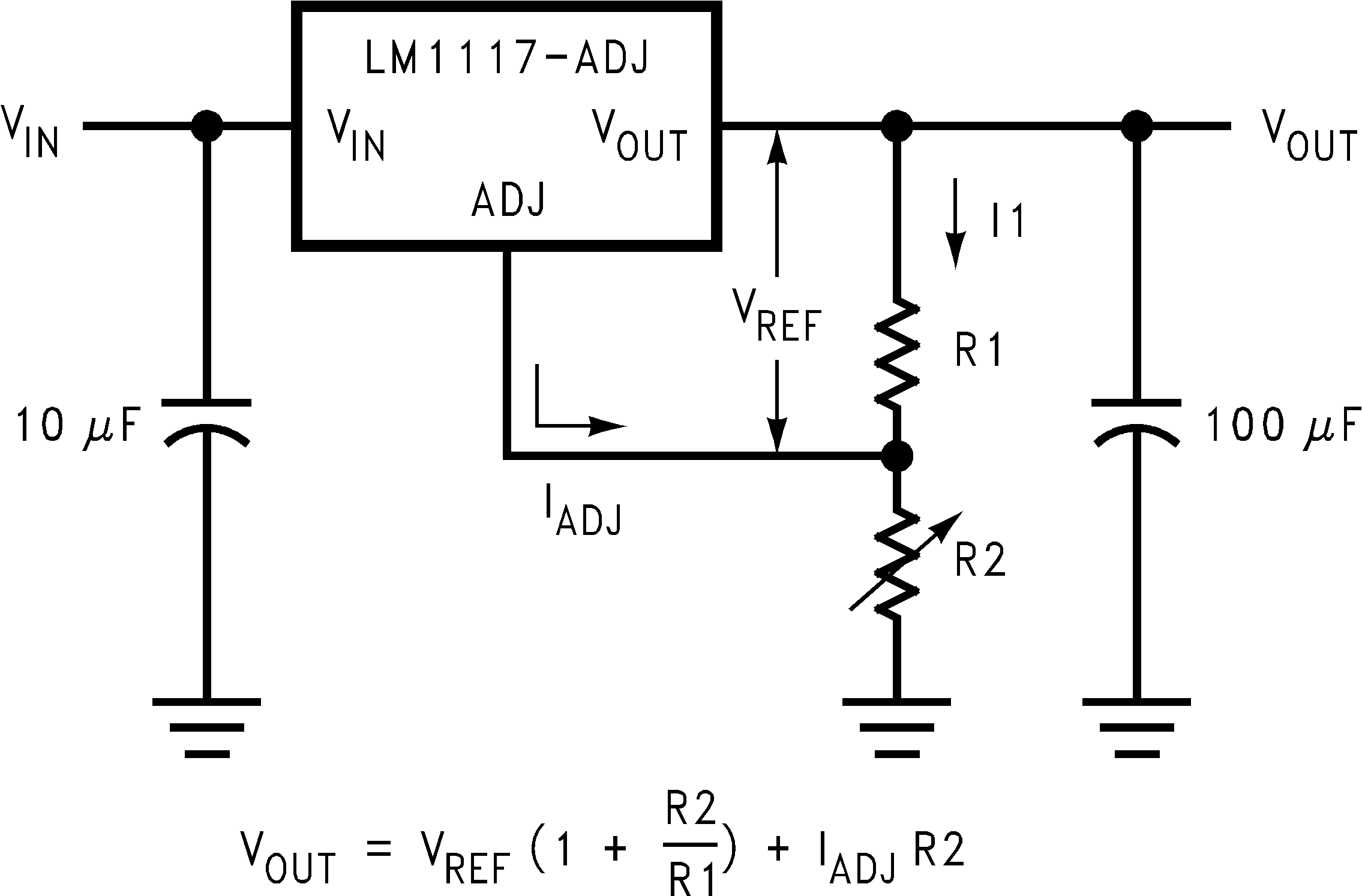
The LM1117 adjustable version develops a 1.25-V reference voltage, VREF, between the output and the adjust pin. As shown in Figure 8-1, this voltage is applied across resistor R1 to generate a constant current I1. The current IADJ from the adjust pin can introduce error to the output, but because this current is very small (60 μA) compared to the I1 and very constant with line and load changes, the error can be ignored. The constant current I1 then flows through the output set resistor R2 and sets the output voltage to the desired level.

For fixed voltage devices, R1 and R2 are integrated inside the devices.
GUID-E10E377F-5D43-4A57-BF0C-5922FDA1B797-low.pngFigure 8-1 Basic Adjustable Regulator