SNLS384G February 1995 – June 2015 LM1881
PRODUCTION DATA.
- 1 Features
- 2 Applications
- 3 Description
- 4 Revision History
- 5 Pin Configuration and Functions
- 6 Specifications
- 7 Detailed Description
- 8 Application and Implementation
- 9 Power Supply Recommendations
- 10Device and Documentation Support
- 11Mechanical, Packaging, and Orderable Information
Package Options
Mechanical Data (Package|Pins)
Thermal pad, mechanical data (Package|Pins)
Orderable Information
6 Specifications
6.1 Absolute Maximum Ratings
over operating free-air temperature range (unless otherwise noted)(1)(3)| MIN | MAX | UNIT | |||
|---|---|---|---|---|---|
| Supply Voltage | 13.2 | V | |||
| Input Voltage | 3 VP-P (VCC = 5) | 6 VP-P (VCC ≥ 8) | V | ||
| Output Sink Currents; Pins, 1, 3, 5 | 5 | mA | |||
| Output Sink Current; Pin 7 | 2 | mA | |||
| Soldering Information | PDIP Package (10 sec.) | 260 | °C | ||
| SOIC Package | Vapor Phase (60 sec.) | 215 | |||
| Infrared (15 sec.) | 220 | ||||
| Storage temperature, Tstg | −65 | 150 | °C | ||
(1) Stresses beyond those listed under Absolute Maximum Ratings may cause permanent damage to the device. These are stress ratings only, which do not imply functional operation of the device at these or any other conditions beyond those indicated under Recommended Operating Conditions. Exposure to absolute-maximum-rated conditions for extended periods may affect device reliability.
(2) For operation in ambient temperatures above 25°C, the device must be derated based on a 150°C maximum junction temperature and a package thermal resistance of 110°C/W, junction to ambient.
(3) If Military/Aerospace specified devices are required, please contact the TI Sales Office/ Distributors for availability and specifications.
6.2 ESD Ratings
| VALUE | UNIT | |||
|---|---|---|---|---|
| V(ESD) | Electrostatic discharge | Human body model (HBM), per ANSI/ESDA/JEDEC JS-001(1) | ±2000 | V |
| Machine Model | ±200 | |||
(1) JEDEC document JEP155 states that 500-V HBM allows safe manufacturing with a standard ESD control process.
6.3 Recommended Operating Conditions
over operating free-air temperature range (unless otherwise noted)| MIN | MAX | UNIT | ||
|---|---|---|---|---|
| TA | Operating free-air temperature | 0 | 70 | °C |
6.4 Electrical Characteristics LM1881
VCC = 5 V; RSET = 680 kΩ; TA = 0°C to +70°C by correlation with 100% electrical testing at TA=25°C| PARAMETER | TEST CONDITIONS | MIN | TYP(1) | MAX | UNIT | |
|---|---|---|---|---|---|---|
| Supply Current | Outputs at Logic 1 |
VCC = 5 V | 5.2 | 10 | mA | |
| VCC = 12 V | 5.5 | 12 | ||||
| DC Input Voltage | Pin 2 | 1.3 | 1.5 | 1.8 | V | |
| Input Threshold Voltage | See (2) | 55 | 70 | 85 | mV | |
| Input Discharge Current | Pin 2; VIN = 2 V | 6 | 11 | 16 | µA | |
| Input Clamp Charge Current | Pin 2; VIN = 1 V | 0.2 | 0.8 | mA | ||
| RSET Pin Reference Voltage | Pin 6;(3) | 1.1 | 1.22 | 1.35 | V | |
| Composite Sync. & Vertical Outputs | IOUT = 40 µA; Logic 1 |
VCC = 5 V | 4.0 | 4.5 | V | |
| VCC = 12 V | 11 | |||||
| IOUT = 1.6 mA Logic 1 |
VCC = 5 V | 2.4 | 3.6 | V | ||
| VCC = 12 V | 10 | |||||
| Burst Gate and Odd and Even Outputs | IOUT = 40 µA; Logic 1 |
VCC = 5 V | 4 | 4.5 | V | |
| VCC = 12 V | 11 | |||||
| Composite Sync. Output | IOUT = −1.6 mA; Logic 0; Pin 1 | 0.2 | 0.8 | V | ||
| Vertical Sync. Output | IOUT = −1.6 mA; Logic 0; Pin 3 | 0.2 | 0.8 | V | ||
| Burst Gate Output | IOUT = −1.6 mA; Logic 0; Pin 5 | 0.2 | 0.8 | V | ||
| Odd and Even Output | IOUT = −1.6 mA; Logic 0; Pin 7 | 0.2 | 0.8 | V | ||
| Vertical Sync Width | 190 | 230 | 300 | µs | ||
| Burst Gate Width | 2.7 kΩ from Pin 5 to VCC | 2.5 | 4 | 4.7 | µs | |
| Vertical Default Time | See (4) | 32 | 65 | 90 | µs | |
(1) Typicals are at TJ = 25°C and represent the most likely parametric norm.
(2) Relative difference between the input clamp voltage and the minimum input voltage which produces a horizontal output pulse.
(3) Careful attention should be made to prevent parasitic capacitance coupling from any output pin (Pins 1, 3, 5 and 7) to the RSET pin (Pin 6).
(4) Delay time between the start of vertical sync (at input) and the vertical output pulse.
6.5 Dissipation Ratings
| MIN | MAX | UNIT | ||
|---|---|---|---|---|
| Package Dissipation(2) | 1100 | mW | ||
6.6 Typical Characteristics
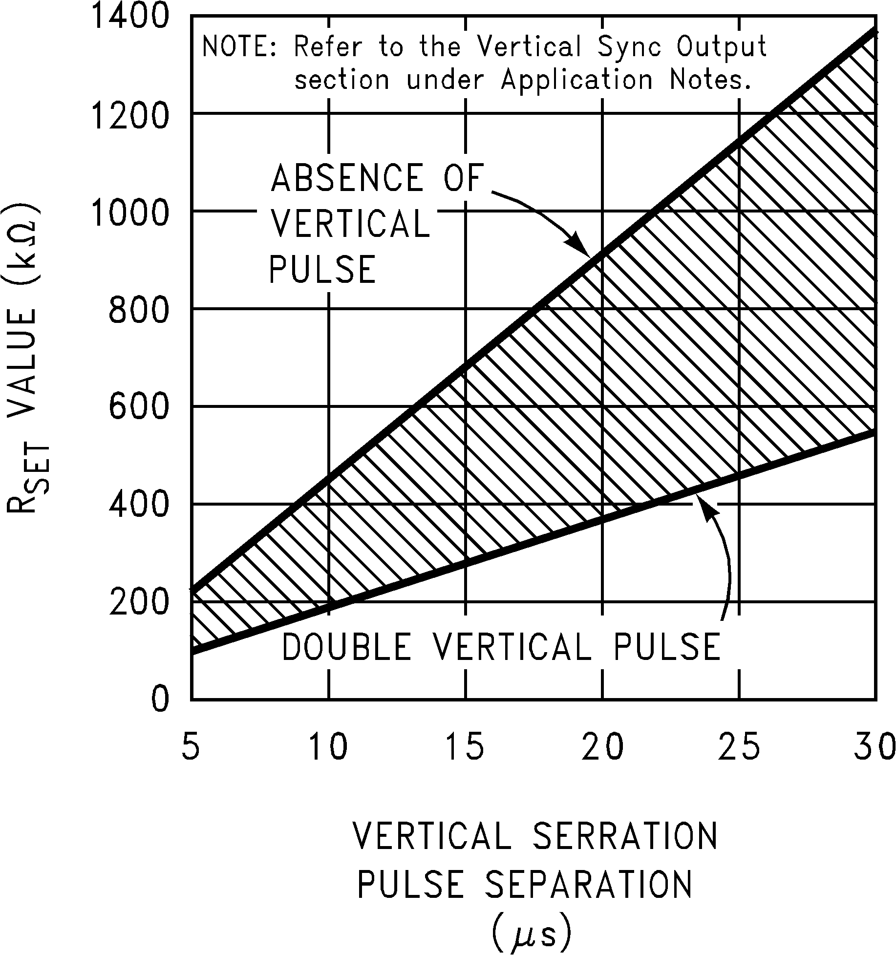 Figure 1. RSET Value Selection vs Vertical Serration Pulse Separation
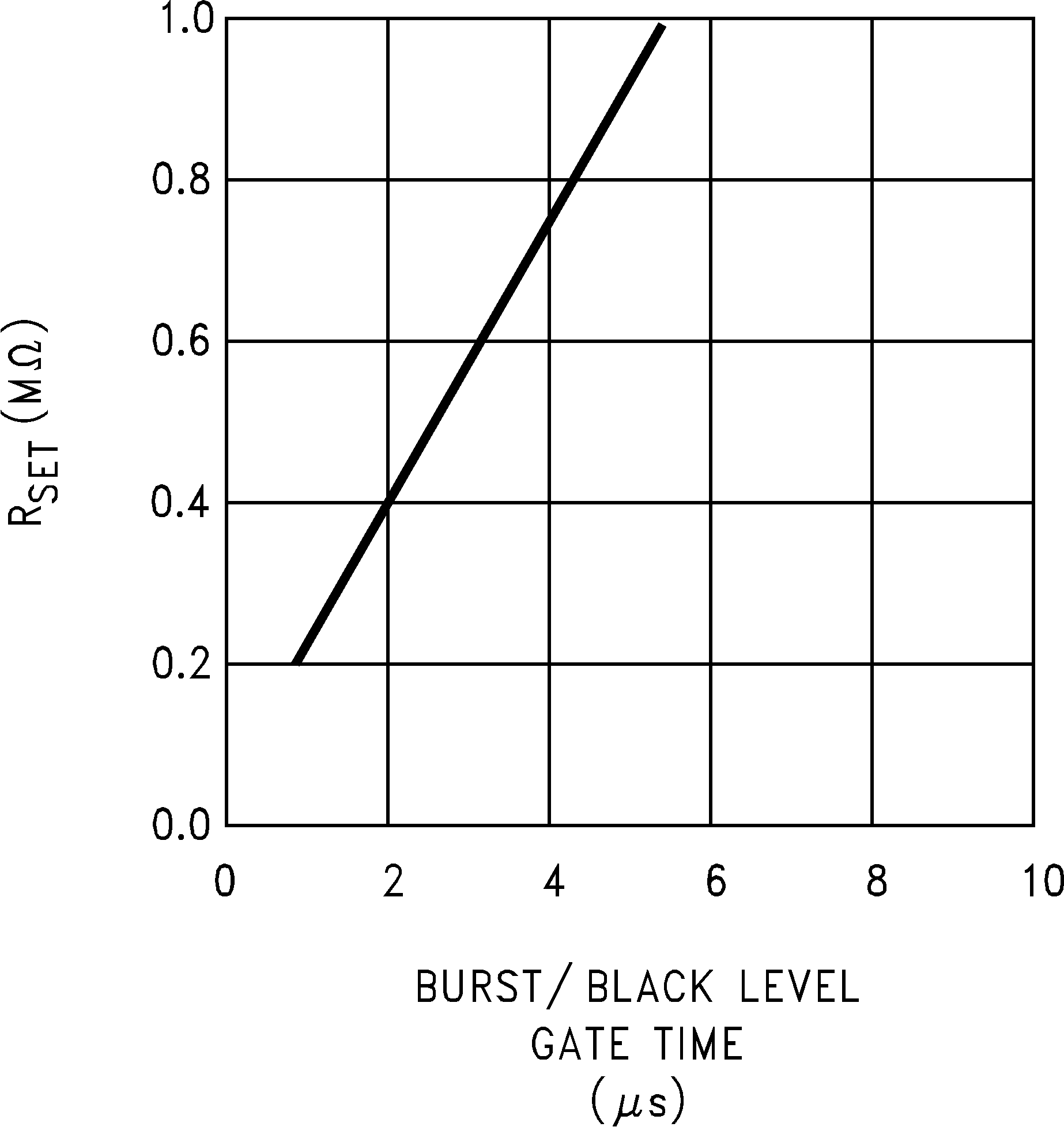 Figure 3. Burst or Black Level Gate Time vs RSET
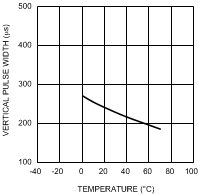 Figure 5. Vertical Pulse Width vs Temperature
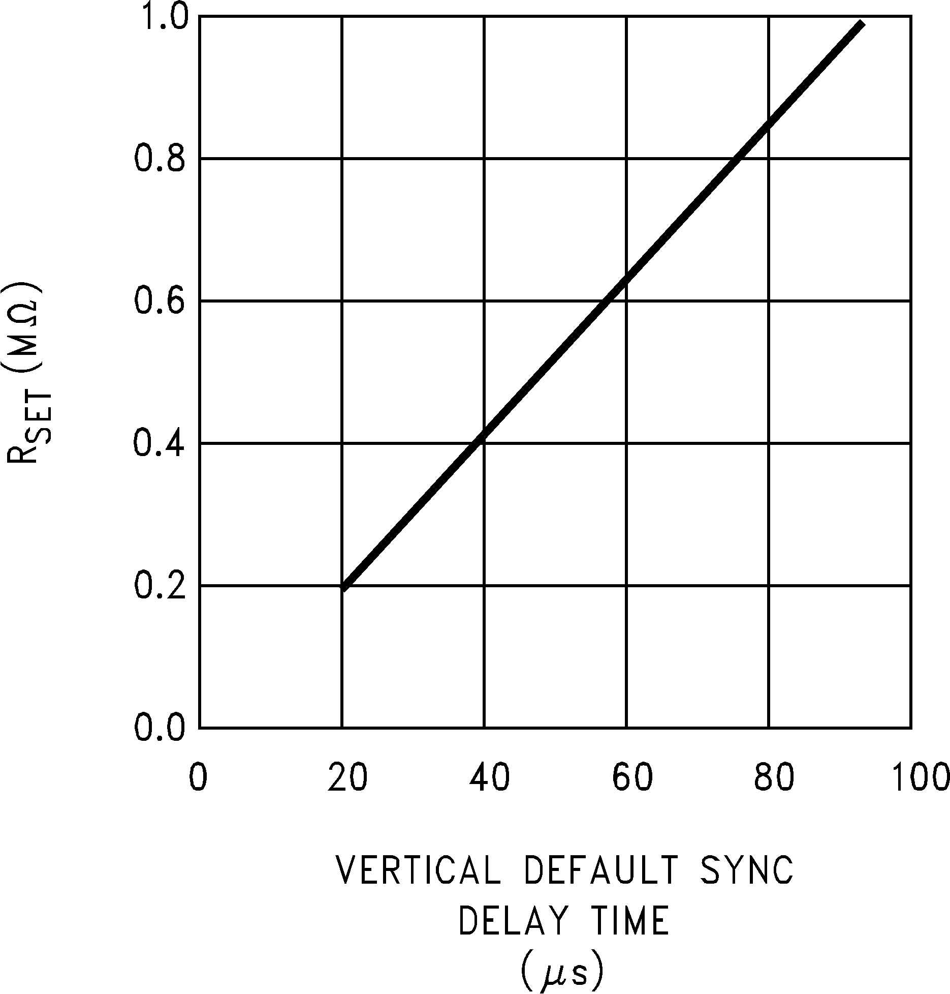 Figure 2. Vertical Default Sync Delay Time vs RSET
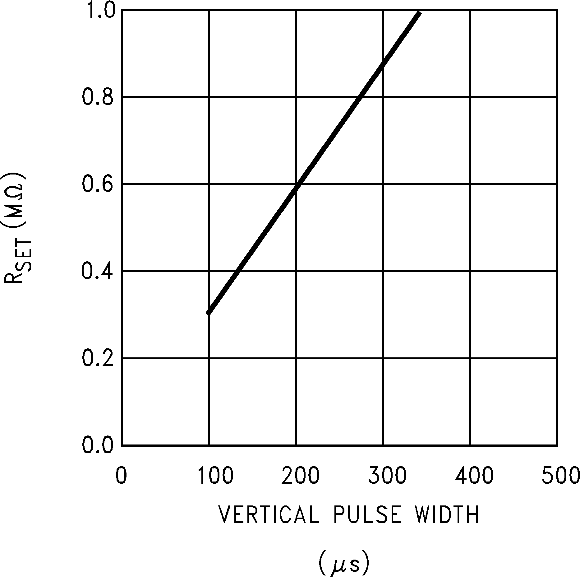 Figure 4. Vertical Pulse Width vs RSET
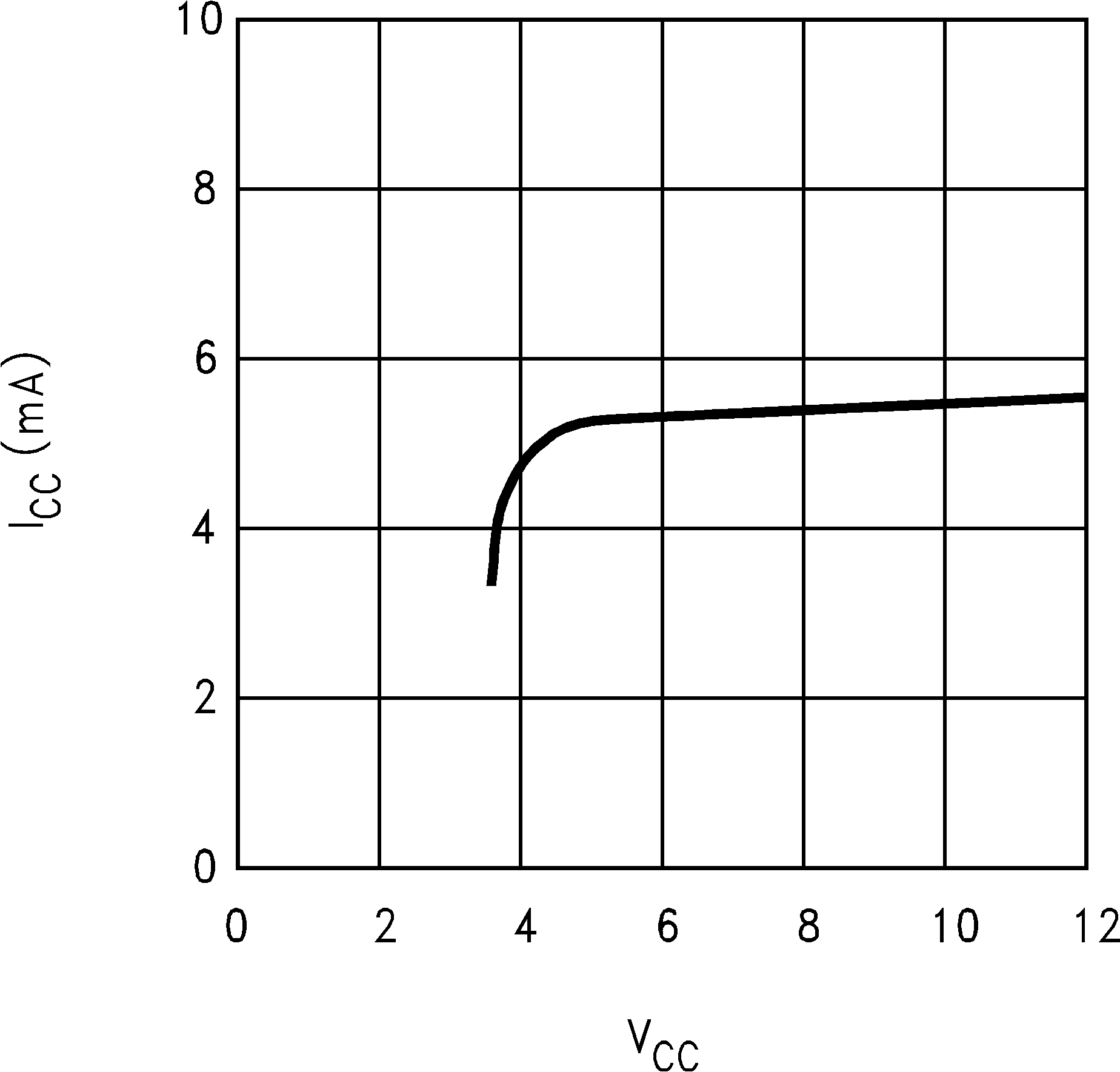 Figure 6. Supply Current vs Supply Voltage