SNIS106Q December 1999 – January 2015 LM20
PRODUCTION DATA.
- 1 Features
- 2 Applications
- 3 Description
- 4 Revision History
- 5 Pin Configuration and Functions
- 6 Specifications
- 7 Detailed Description
- 8 Application and Implementation
- 9 Power Supply Recommendations
- 10Layout
- 11Device and Documentation Support
- 12Mechanical, Packaging, and Orderable Information
Package Options
Mechanical Data (Package|Pins)
Thermal pad, mechanical data (Package|Pins)
Orderable Information
8 Application and Implementation
NOTE
Information in the following applications sections is not part of the TI component specification, and TI does not warrant its accuracy or completeness. TI’s customers are responsible for determining suitability of components for their purposes. Customers should validate and test their design implementation to confirm system functionality.
8.1 Application Information
The LM20 features make it suitable for many general temperature sensing applications. Multiple package options expand on its, flexibility.
8.1.1 Capacitive Loads
The LM20 handles capacitive loading well. Without any precautions, the LM20 can drive any capacitive load less than 300 pF as shown in Figure 2. Over the specified temperature range the LM20 has a maximum output impedance of 160 Ω. In an extremely noisy environment, it may be necessary to add some filtering to minimize noise pickup. It is recommended that 0.1 μF be added from V+ to GND to bypass the power supply voltage, as shown in Figure 4. In a noisy environment, it may even be necessary to add a capacitor from the output to ground with a series resistor as shown in Figure 4. A 1-μF output capacitor with the 160-Ω maximum output impedance and a 200-Ω series resistor will form a 442-Hz lowpass filter. Because the thermal time constant of the LM20 is much slower, the overall response time of the LM20 will not be significantly affected.
In situations where a transient load current is placed on the circuit output the series resistance value may be increased to compensate for any ringing that may be observed.
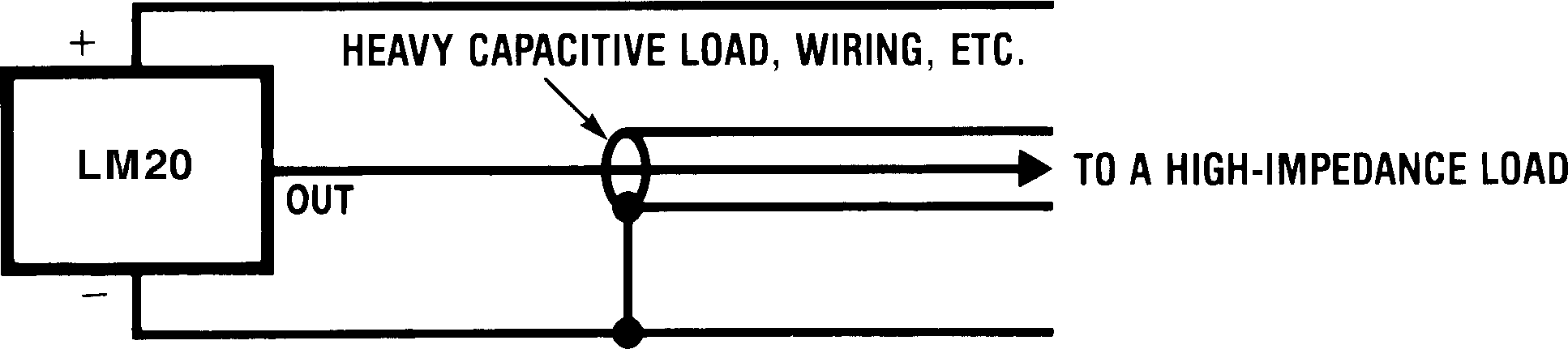 Figure 2. LM20 No Decoupling Required for Capacitive Loads Less Than 300 pF
Table 2. Capacitive Loading Isolation
| Minimum R (Ω) | C (µF) |
|---|---|
| 200 | 1 |
| 470 | 0.1 |
| 680 | 0.01 |
| 1 k | 0.001 |
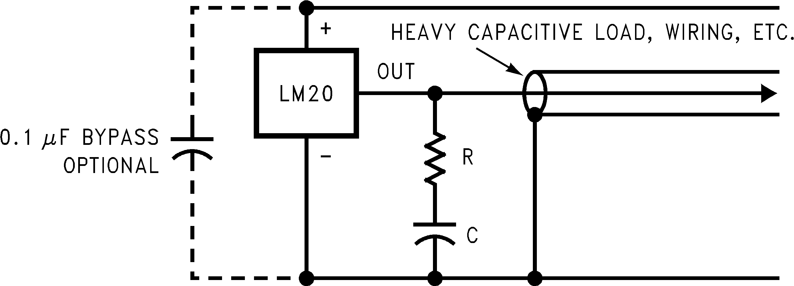 Figure 3. LM20 With Compensation for Capacitive Loading Greater Than 300 pF
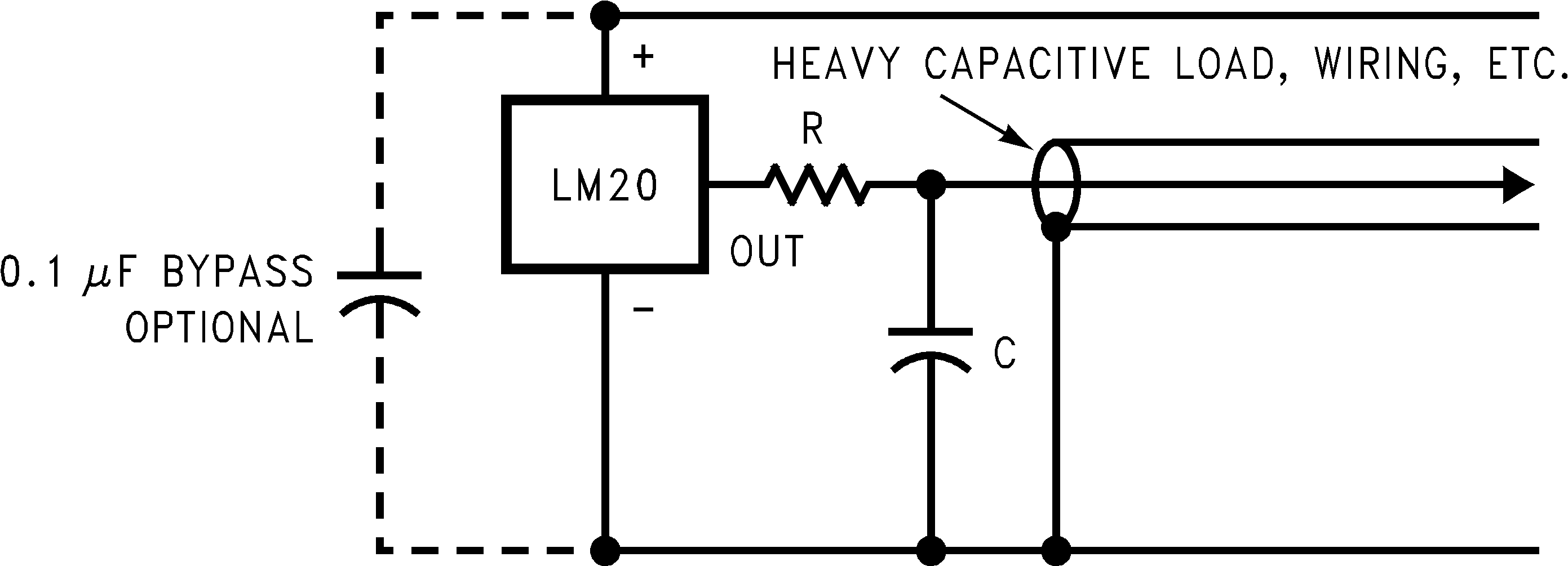 Figure 4. LM20 With Filter for Noisy Environment and Capacitive Loading Greater Than 300 pF
NOTE
Either placement of resistor, as shown in Figure 3 and Figure 4, is just as effective.
8.1.2 LM20 DSBGA Light Sensitivity
Exposing the LM20 DSBGA package to bright sunlight may cause the output reading of the LM20 to drop by
1.5 V. In a normal office environment of fluorescent lighting the output voltage is minimally affected (less than a millivolt drop). In either case, TI recommends that the LM20 DSBGA be placed inside an enclosure of some type that minimizes its light exposure. Most chassis provide more than ample protection. The LM20 does not sustain permanent damage from light exposure. Removing the light source will cause the output voltage of the LM20 to recover to the proper value.
8.2 Typical Applications
8.2.1 Full-Range Celsius (Centigrade) Temperature Sensor (−55°C to 130°C) Operating from a Single Li-Ion Battery Cell
The LM20 has a very low supply current and a wide supply range; therefore, it can easily be driven by a battery as shown in Figure 5.
 Figure 5. Full-Range Celsius (Centigrade) Temperature Sensor (−55°C To 130°C) Operating from a Single Li-Ion Battery Cell
8.2.1.1 Design Requirements
Because the LM20 is a simple temperature sensor that provides an analog output, design requirements related to layout are more important than electrical requirements. Refer to the Layout section for a detailed description.
8.2.1.2 Detailed Design Procedure
The LM20 transfer function can be described in different ways with varying levels of precision. A simple linear transfer function with good accuracy near 25°C is:
Over the full operating temperature range of −55°C to 130°C, best accuracy can be obtained by using the parabolic transfer function.
Solving Equation 5 for T:
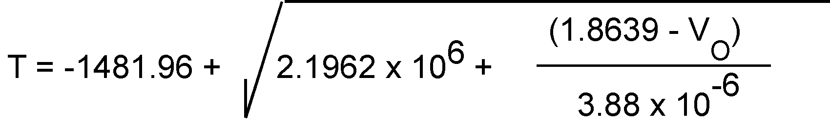
An alternative to the quadratic equation a second order transfer function can be determined using the least-squares method:
where
- T is temperature express in °C and VO is the output voltage expressed in volts.
A linear transfer function can be used over a limited temperature range by calculating a slope and offset that give best results over that range. A linear transfer function can be calculated from the parabolic transfer function of the LM20. The slope of the linear transfer function can be calculated using the Equation 8 equation:
where
- T is the middle of the temperature range of interest and m is in V/°C.
For example for the temperature range of TMIN = −30 to TMAX = 100°C:
and
The offset of the linear transfer function can be calculated using the Equation 11 equation:
where
- VOP(TMAX) is the calculated output voltage at TMAX using the parabolic transfer function for VO
- VOP(T) is the calculated output voltage at T using the parabolic transfer function for VO.
The best fit linear transfer function for many popular temperature ranges was calculated in Table 3. As shown in Table 3, the error introduced by the linear transfer function increases with wider temperature ranges.
Table 3. First Order Equations Optimized for Different Temperature Ranges
| Temperature Range | Linear Equation | Maximum Deviation of Linear Equation from Parabolic Equation (°C) | |
|---|---|---|---|
| Tmin (°C) | Tmax (°C) | ||
| −55 | 130 | VO = −11.79 mV/°C × T + 1.8528 V | ±1.41 |
| −40 | 110 | VO = −11.77 mV/°C × T + 1.8577 V | ±0.93 |
| −30 | 100 | VO = −11.77 mV/°C × T + 1.8605 V | ±0.70 |
| -40 | 85 | VO = −11.67 mV/°C × T + 1.8583 V | ±0.65 |
| −10 | 65 | VO = −11.71 mV/°C × T + 1.8641 V | ±0.23 |
| 35 | 45 | VO = −11.81 mV/°C × T + 1.8701 V | ±0.004 |
| 20 | 30 | VO = –11.69 mV/°C × T + 1.8663 V | ±0.004 |
Table 4. Output Voltage vs Temperature
| Temperature (T) | Typical VO |
|---|---|
| 130°C | 303 mV |
| 100°C | 675 mV |
| 80°C | 919 mV |
| 30°C | 1515 mV |
| 25°C | 1574 mV |
| 0°C | 1863.9 mV |
| –30°C | 2205 mV |
| −40°C | 2318 mV |
| −55°C | 2485 mV |
8.2.1.3 Application Curve
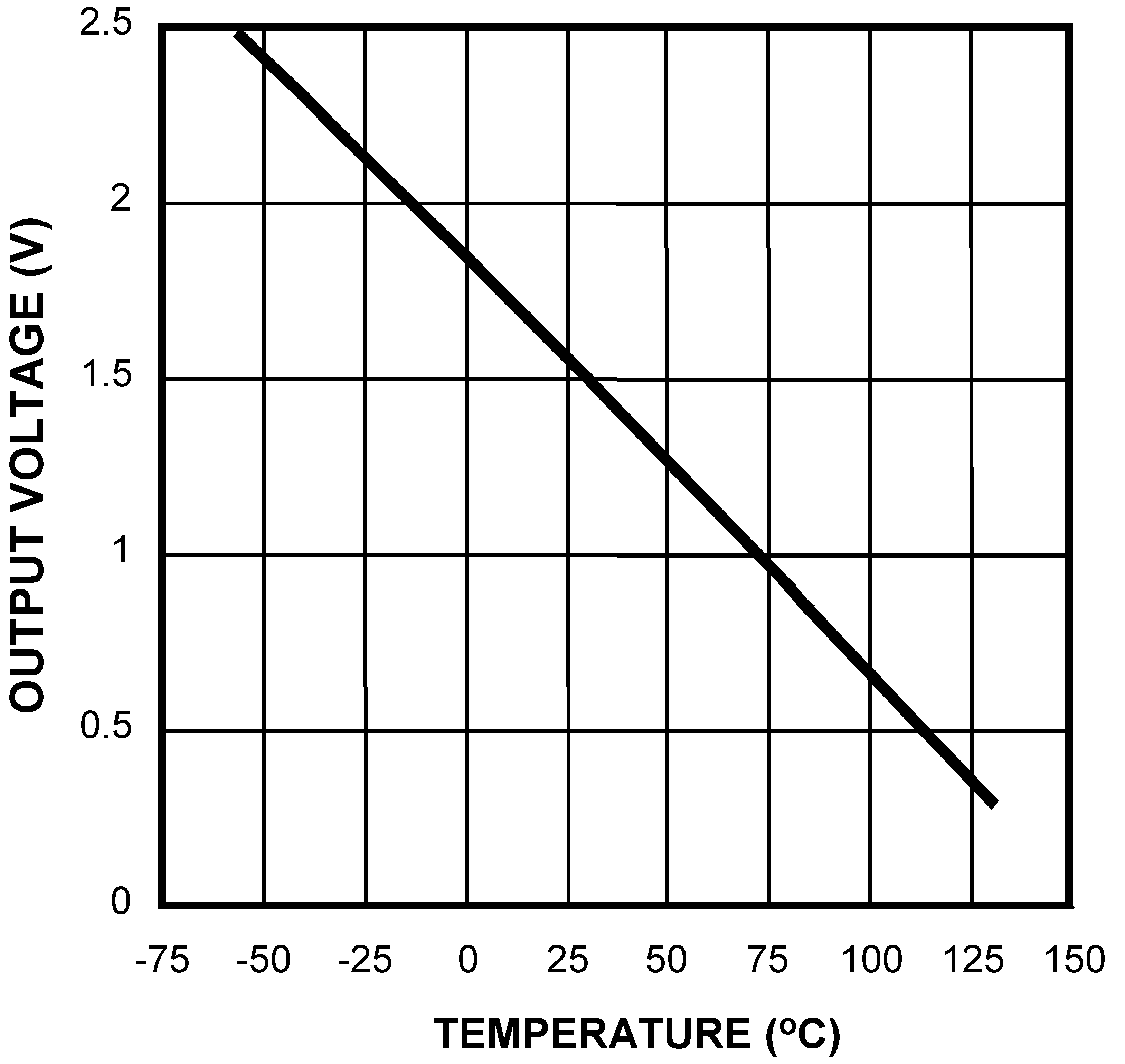 Figure 6. Output Voltage vs Temperature
8.2.2 Centigrade Thermostat
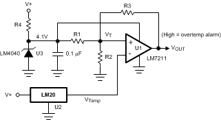 Figure 7. Centigrade Thermostat
8.2.2.1 Design Requirements
A simple thermostat can be created by using a reference (LM4040) and a comparator (LM7211) as shown in Figure 7.
8.2.2.2 Detailed Design Procedure
The threshold values can be calculated using Equation 12 and Equation 13.


8.2.2.3 Application Curve
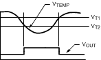 Figure 8. Thermostat Output Waveform
8.3 System Examples
8.3.1 Conserving Power Dissipation With Shutdown
The LM20 draws very little power; therefore, it can simply be shutdown by driving its supply pin with the output of an logic gate as shown in Figure 9.
 Figure 9. Conserving Power Dissipation With Shutdown
8.3.2 Analog-to-Digital Converter Input Stage
Most CMOS ADCs found in ASICs have a sampled data comparator input structure that is notorious for causing grief to analog output devices such as the LM20 and many operational amplifiers. The cause of this grief is the requirement of instantaneous charge of the input sampling capacitor in the ADC. This requirement is easily accommodated by the addition of a capacitor. Because not all ADCsFigure 10 have identical input stages, the charge requirements will vary necessitating a different value of compensating capacitor. This ADC is shown as an example only. If a digital output temperature is required, refer to devices such as the LM74.
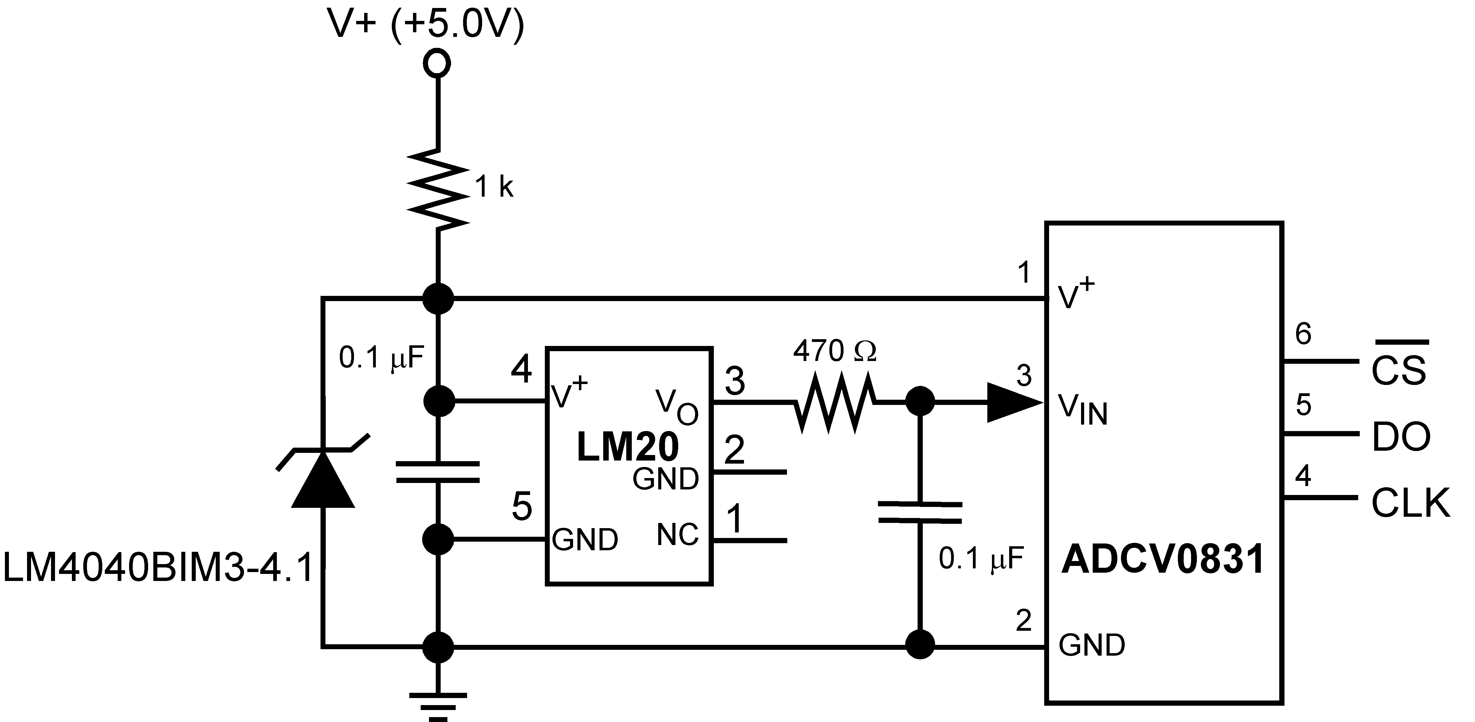 Figure 10. Suggested Connection to a Sampling Analog to Digital Converter Input Stage