SNVS591L September 2008 – November 2014 LM22675 , LM22675-Q1
PRODUCTION DATA.
- 1 Features
- 2 Applications
- 3 Description
- 4 Revision History
- 5 Pin Configuration and Functions
- 6 Specifications
- 7 Detailed Description
- 8 Application and Implementation
- 9 Power Supply Recommendations
- 10Layout
- 11Device and Documentation Support
- 12Mechanical, Packaging, and Orderable Information
Package Options
Mechanical Data (Package|Pins)
- DDA|8
Thermal pad, mechanical data (Package|Pins)
- DDA|8
Orderable Information
7 Detailed Description
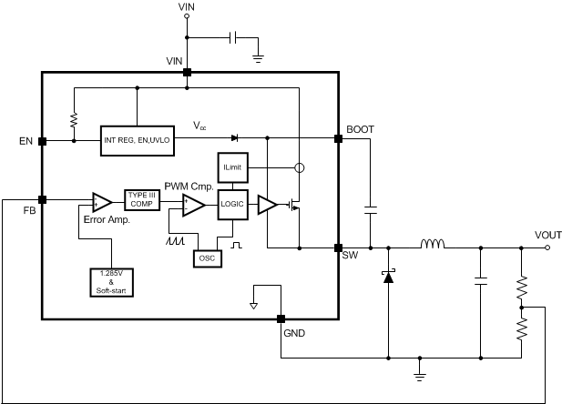
7.1 Overview
The LM22675 incorporates a voltage mode constant frequency PWM architecture. In addition, input voltage feedforward is used to stabilize the loop gain against variations in input voltage. This allows the loop compensation to be optimized for transient performance. The power MOSFET, in conjunction with the diode, produce a rectangular waveform at the switch pin, that swings from about zero volts to VIN. The inductor and output capacitor average this waveform to become the regulator output voltage. By adjusting the duty cycle of this waveform, the output voltage can be controlled. The error amplifier compares the output voltage with the internal reference and adjusts the duty cycle to regulate the output at the desired value.
The internal loop compensation of the -ADJ option is optimized for outputs of 5 V and below. If an output voltage of 5 V or greater is required, the -5.0 option can be used with an external voltage divider. The minimum output voltage is equal to the reference voltage, that is, 1.285 V (typ).
7.2 Functional Block Diagram
7.3 Feature Description
7.3.1 Precision Enable and UVLO
The precision enable input (EN) is used to control the regulator. The precision feature allows simple sequencing of multiple power supplies with a resistor divider from another supply. Connecting this pin to ground or to a voltage less than 1.6 V (typ) will turn off the regulator. The current drain from the input supply, in this state, is 25 µA (typ) at an input voltage of 12 V. The EN input has an internal pullup of about 6 µA. Therefore this pin can be left floating or pulled to a voltage greater than 2.2 V (typ) to turn the regulator on. The hysteresis on this input is about 0.6 V (typ) above the 1.6 V (typ) threshold. When driving the enable input, the voltage must never exceed the 6 V absolute maximum specification for this pin.
Although an internal pullup is provided on the EN pin, it is good practice to pull the input high, when this feature is not used, especially in noisy environments. This can most easily be done by connecting a resistor between VIN and the EN pin. The resistor is required, because the internal zener diode, at the EN pin, will conduct for voltages above about 6 V. The current in this zener must be limited to less than 100 µA. A resistor of 470 kΩ will limit the current to a safe value for input voltages as high 42 V. Smaller values of resistor can be used at lower input voltages.
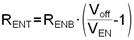
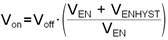
The LM22675 device also incorporates an input undervoltage lock-out (UVLO) feature. This prevents the regulator from turning on when the input voltage is not great enough to properly bias the internal circuitry. The rising threshold is 4.3 V (typ) while the falling threshold is 3.9 V (typ). In some cases these thresholds may be too low to provide good system performance. The solution is to use the EN input as an external UVLO to disable the part when the input voltage falls below a lower boundary. This is often used to prevent excessive battery discharge or early turn-on during start-up. This method is also recommended to prevent abnormal device operation in applications where the input voltage falls below the minimum of 4.5 V. Figure 10 shows the connections to implement this method of UVLO. Equation 1 and Equation 2 can be used to determine the correct resistor values.
Where:
Voff is the input voltage where the regulator shuts off.
Von is the voltage where the regulator turns on.
Due to the 6 µA pullup, the current in the divider should be much larger than this. A value of 20 kΩ, for RENB is a good first choice. Also, a zener diode may be needed between the EN pin and ground, in order to comply with the absolute maximum ratings on this pin.
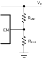 Figure 10. External UVLO Connections
7.3.2 Soft-Start
The soft-start feature allows the regulator to gradually reach steady-state operation, thus reducing start-up stresses. The internal soft-start feature brings the output voltage up in about 500 µs. This time is fixed and can not be changed. Soft-start is reset any time the part is shut down or a thermal overload event occurs.
7.3.3 Boot-Strap Supply
The LM22675 incorporates a floating high-side gate driver to control the power MOSFET. The supply for this driver is the external boot-strap capacitor connected between the BOOT pin and SW. A good quality 10 nF ceramic capacitor must be connected to these pins with short, wide PCB traces. One reason the regulator imposes a minimum off-time is to ensure that this capacitor recharges every switching cycle. A minimum load of about 5 mA is required to fully recharge the boot-strap capacitor in the minimum off-time. Some of this load can be provided by the output voltage divider, if used.
7.3.4 Internal Loop Compensation
The LM22675 has internal loop compensation designed to provide a stable regulator over a wide range of external power stage components.
The internal compensation of the -ADJ option is optimized for output voltages below 5 V. If an output voltage of
5 V or greater is needed, the -5.0 option with an external resistor divider can be used.
Ensuring stability of a design with a specific power stage (inductor and output capacitor) can be tricky. The LM22675 stability can be verified using the WEBENCH Designer online circuit simulation tool. A quick start spreadsheet can also be downloaded from the online product folder.
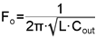
The complete transfer function for the regulator loop is found by combining the compensation and power stage transfer functions. The LM22675 has internal type III loop compensation, as detailed in Figure 11. This is the approximate "straight line" function from the FB pin to the input of the PWM modulator. The power stage transfer function consists of a dc gain and a second order pole created by the inductor and output capacitor(s). Due to the input voltage feedforward employed in the LM22675, the power stage dc gain is fixed at 20 dB. The second order pole is characterized by its resonant frequency and its quality factor (Q). For a first pass design, the product of inductance and output capacitance should conform to Equation 3.
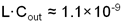
Alternatively, this pole should be placed between 1.5 kHz and 15 kHz and is given by Equation 4.
The Q factor depends on the parasitic resistance of the power stage components and is not typically in the control of the designer. Of course, loop compensation is only one consideration when selecting power stage components; see Application and Implementation for more details.
 Figure 11. Compensator Gain
In general, hand calculations or simulations can only aid in selecting good power stage components. Good design practice dictates that load and line transient testing should be done to verify the stability of the application. Also, Bode plot measurements should be made to determine stability margins. AN-1889 How to Measure the Loop Transfer Function of Power Supplies (SNVA364) shows how to perform a loop transfer function measurement with only an oscilloscope and function generator.
7.4 Device Functional Modes
7.4.1 Current Limit
The LM22675 has current limiting to prevent the switch current from exceeding safe values during an accidental overload on the output. This peak current limit is found in the Electrical Characteristics table under the heading of ICL. The maximum load current that can be provided, before current limit is reached, is determined from Equation 5.
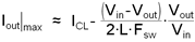
Where:
L is the value of the power inductor.
When the LM22675 enters current limit, the output voltage will drop and the peak inductor current will be fixed at ICL at the end of each cycle. The switching frequency will remain constant while the duty cycle drops. The load current will not remain constant, but will depend on the severity of the overload and the output voltage.
For very severe overloads ("short-circuit"), the regulator changes to a low frequency current foldback mode of operation. The frequency foldback is about 1/5 of the nominal switching frequency. This will occur when the current limit trips before the minimum on-time has elapsed. This mode of operation is used to prevent inductor current "run-away", and is associated with very low output voltages when in overload. Equation 6 can be used to determine what level of output voltage will cause the part to change to low frequency current foldback.
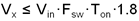
Where:
Fsw is the normal switching frequency.
Vin is the maximum for the application.
If the overload drives the output voltage to less than or equal to Vx, the part will enter current foldback mode. If a given application can drive the output voltage to ≤Vx, during an overload, then a second criterion must be checked. Equation 7 gives the maximum input voltage, when in this mode, before damage occurs.
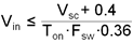
Where:
Vsc is the value of output voltage during the overload.
fsw is the normal switching frequency.
NOTE
If the input voltage should exceed this value, while in foldback mode, the regulator and/or the diode may be damaged.
It is important to note that the voltages in these equations are measured at the inductor. Normal trace and wiring resistance will cause the voltage at the inductor to be higher than that at a remote load. Therefore, even if the load is shorted with zero volts across its terminals, the inductor will still see a finite voltage. It is this value that should be used for Vx and Vsc in the calculations. In order to return from foldback mode, the load must be reduced to a value much lower than that required to initiate foldback. This load "hysteresis" is a normal aspect of any type of current limit foldback associated with voltage regulators.
The safe operating area, when in short circuit mode, is shown in Figure 12. Operating points below and to the right of the curve represent safe operation.
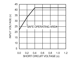 Figure 12. SOA
7.4.2 Thermal Protection
Internal thermal shutdown circuitry protects the LM22675 should the maximum junction temperature be exceeded. This protection is activated at about 150°C, with the result that the regulator will shutdown until the temperature drops below about 135°C.
7.4.3 Duty Cycle Limits
Ideally the regulator would control the duty cycle over the full range of zero to one. However due to inherent delays in the circuitry, there are limits on both the maximum and minimum duty cycles that can be reliably controlled. This in turn places limits on the maximum and minimum input and output voltages that can be converted by the LM22675. A minimum on-time is imposed by the regulator in order to correctly measure the switch current during a current limit event. A minimum off-time is imposed in order the re-charge the bootstrap capacitor. Equation 8 can be used to determine the approximate maximum input voltage for a given output voltage.
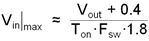
Where:
Fsw is the switching frequency.
TON is the minimum on-time.
Both parameters are found in the Electrical Characteristics table.
The worst case occurs at the lowest output voltage. If the input voltage, found in Equation 8, is exceeded, the regulator will skip cycles; thus, effectively lowering the switching frequency. The consequences of this are higher output voltage ripple and a degradation of the output voltage accuracy.
The second limitation is the maximum duty cycle before the output voltage will "dropout" of regulation. Equation 9 can be used to approximate the minimum input voltage before dropout occurs.

Where:
The values of TOFF and RDS(ON) are found in the Electrical Characteristics table.
The worst case here occurs at the highest load. In this equation, RL is the dc inductor resistance. Of course, the lowest input voltage to the regulator must not be less than 4.5 V (typ).