SNVS585M September 2008 – October 2020 LM22678 , LM22678-Q1
PRODUCTION DATA
- 1 Features
- 2 Applications
- 3 Description
- 4 Revision History
- 5 Pin Configuration and Functions
- 6 Specifications
- 7 Detailed Description
- 8 Application and Implementation
- 9 Layout
- 10Device and Documentation Support
Package Options
Mechanical Data (Package|Pins)
- NDR|7
Thermal pad, mechanical data (Package|Pins)
Orderable Information
8.1.1 Output Voltage Divider Selection
For output voltages between about 1.285 V and 5 V, the -ADJ option should be used, with an appropriate voltage divider as shown in Figure 8-1. Equation 10 can be used to calculate the resistor values of this divider.
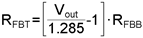
A good value for RFBB is 1 kΩ. This will help to provide some of the minimum load current requirement and reduce susceptibility to noise pick-up. The top of RFBT should be connected directly to the output capacitor or to the load for remote sensing. If the divider is connected to the load, a local high-frequency bypass should be provided at that location.
For output voltages of 5 V, the -5.0 option should be used. In this case no divider is needed and the FB pin is connected to the output. The approximate values of the internal voltage divider are as follows: 7.38 kΩ from the FB pin to the input of the error amplifier and 2.55 kΩ from there to ground.
Both the -ADJ and -5.0 options can be used for output voltages greater than 5 V, by using the correct output divider. As mentioned in Section 7.3.4, the -5.0 option is optimized for output voltages of 5 V. However, for output voltages greater than 5 V, this option may provide better loop bandwidth than the -ADJ option, in some applications. If the -5.0 option is to be used at output voltages greater than 5 V, Equation 11 should be used to determine the resistor values in the output divider.
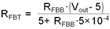
Again, a value of RFBB of about 1 kΩ is a good first choice.
 Figure 8-1 Resistive Feedback Divider
A maximum value of 10 kΩ is recommended for the sum of RFBB and RFBT to maintain good output voltage accuracy for the -ADJ option. A maximum of 2 kΩ is recommended for the -5.0 option. For the -5.0 option, the total internal divider resistance is typically 9.93 kΩ.
In all cases the output voltage divider should be placed as close as possible to the FB pin of the LM22678 device; because this is a high impedance input and is susceptible to noise pick-up.