SNVS585M September 2008 – October 2020 LM22678 , LM22678-Q1
PRODUCTION DATA
- 1 Features
- 2 Applications
- 3 Description
- 4 Revision History
- 5 Pin Configuration and Functions
- 6 Specifications
- 7 Detailed Description
- 8 Application and Implementation
- 9 Layout
- 10Device and Documentation Support
Package Options
Mechanical Data (Package|Pins)
- NDR|7
Thermal pad, mechanical data (Package|Pins)
Orderable Information
7.4.3 Current Limit
The LM22678 device has current limiting to prevent the switch current from exceeding safe values during an accidental overload on the output. This peak current limit is found in Section 6.6 under the heading of ICL. The maximum load current that can be provided, before current limit is reached, is determined from Equation 5.
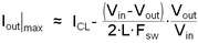
where
- L is the value of the power inductor.
When the LM22678 device enters current limit, the output voltage will drop and the peak inductor current will be fixed at ICL at the end of each cycle. The switching frequency will remain constant while the duty cycle drops. The load current will not remain constant, but will depend on the severity of the overload and the output voltage.
For very severe overloads "short-circuit", the regulator changes to a low frequency current foldback mode of operation. The frequency foldback is about 1/5 of the nominal switching frequency. This will occur when the current limit trips before the minimum on-time has elapsed. This mode of operation is used to prevent inductor current "run-away", and is associated with very low output voltages when in overload. Equation 6 can be used to determine what level of output voltage will cause the part to change to low frequency current foldback.
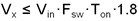
where
- Fsw is the normal switching frequency.
- Vin is the maximum for the application.
If the overload drives the output voltage to less than or equal to Vx, the part will enter current foldback mode. If a given application can drive the output voltage to ≤ Vx, during an overload, then a second criterion must be checked. Equation 7 determines the maximum input voltage, when in this mode, before damage occurs.
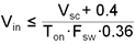
where
- Vsc is the value of output voltage during the overload.
- Fsw is the normal switching frequency.
If the input voltage should exceed this value while in foldback mode, the regulator, diode, or both can be damaged.
It is important to note that the voltages in these equations are measured at the inductor. Normal trace and wiring resistance will cause the voltage at the inductor to be higher than that at a remote load. Therefore, even if the load is shorted with zero volts across its terminals, the inductor will still see a finite voltage. It is this value that should be used for Vx and Vsc in the calculations. In order to return from foldback mode, the load must be reduced to a value much lower than that required to initiate foldback. This load "hysteresis" is a normal aspect of any type of current limit foldback associated with voltage regulators.
The safe operating area, when in short circuit mode, is shown in Figure 7-3. Operating points below and to the right of the curve represent safe operation.
 Figure 7-3 SOA