SNVS585M September 2008 – October 2020 LM22678 , LM22678-Q1
PRODUCTION DATA
- 1 Features
- 2 Applications
- 3 Description
- 4 Revision History
- 5 Pin Configuration and Functions
- 6 Specifications
- 7 Detailed Description
- 8 Application and Implementation
- 9 Layout
- 10Device and Documentation Support
Package Options
Mechanical Data (Package|Pins)
- NDR|7
Thermal pad, mechanical data (Package|Pins)
Orderable Information
8.2.1.2.1.1 Inductor
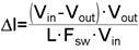
The inductor value is determined based on the load current, ripple current, and the minimum and maximum input voltages. To keep the application in continuous conduction mode (CCM), the maximum ripple current, IRIPPLE, should be less than twice the minimum load current. The general rule of keeping the inductor current peak-to-peak ripple around 30% of the nominal output current is a good compromise between excessive output voltage ripple and excessive component size and cost. Using this value of ripple current, the value of inductor (L) is calculated using Equation 12.
where
- Fsw is the switching frequency.
- Vin should be taken at its maximum value, for the given application.
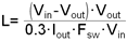
Equation 12 provides a guide to select the value of the inductor L; the nearest standard value will then be used in the circuit.
Once the inductor is selected, the actual ripple current can be determined by Equation 13.
Increasing the inductance will generally slow down the transient response but reduce the output voltage ripple. Reducing the inductance will generally improve the transient response but increase the output voltage ripple.
The inductor must be rated for the peak current, IPK, in a given application, to prevent saturation. During normal loading conditions, the peak current is equal to the load current plus 1/2 of the inductor ripple current.
During an overload condition, as well as during certain load transients, the controller can trip current limit. In this case the peak inductor current is given by ICL, found in Section 6.6. Good design practice requires that the inductor rating be adequate for this overload condition.
If the inductor is not rated for the maximum expected current, it can saturate resulting in damage to the LM22678, the power diode, or both.