SNVS953G December 2012 – May 2021 LM25018
PRODUCTION DATA
- 1 Features
- 2 Applications
- 3 Description
- 4 Revision History
- 5 Pin Configuration and Functions
- 6 Specifications
-
7 Detailed Description
- 7.1 Overview
- 7.2 Functional Block Diagram
- 7.3
Feature Description
- 7.3.1 Control Overview
- 7.3.2 VCC Regulator
- 7.3.3 Regulation Comparator
- 7.3.4 Overvoltage Comparator
- 7.3.5 On-Time Generator
- 7.3.6 Current Limit
- 7.3.7 N-Channel Buck Switch and Driver
- 7.3.8 Synchronous Rectifier
- 7.3.9 Undervoltage Detector
- 7.3.10 Thermal Protection
- 7.3.11 Ripple Configuration
- 7.3.12 Soft Start
- 7.4 Device Functional Modes
-
8 Application and Implementation
- 8.1 Application Information
- 8.2
Typical Applications
- 8.2.1 Application Circuit: 12.5-V to 48-V Input and 10-V, 325-mA Output Buck Converter
- 8.2.2 Application Curves
- 8.2.3
Typical Isolated DC-DC Converter Using LM25018
- 8.2.3.1 Design Requirements
- 8.2.3.2
Detailed Design Procedure
- 8.2.3.2.1 Transformer Turns Ratio
- 8.2.3.2.2 Total IOUT
- 8.2.3.2.3 RFB1, RFB2
- 8.2.3.2.4 Frequency Selection
- 8.2.3.2.5 Transformer Selection
- 8.2.3.2.6 Primary Output Capacitor
- 8.2.3.2.7 Secondary Output Capacitor
- 8.2.3.2.8 Type III Feedback Ripple Circuit
- 8.2.3.2.9 Secondary Diode
- 8.2.3.2.10 VCC and Bootstrap Capacitor
- 8.2.3.2.11 Input Capacitor
- 8.2.3.2.12 UVLO Resistors
- 8.2.3.2.13 VCC Diode
- 8.2.3.3 Application Curves
- 9 Power Supply Recommendations
- 10Layout
- 11Device and Documentation Support
- 12Mechanical, Packaging, and Orderable Information
Package Options
Mechanical Data (Package|Pins)
Thermal pad, mechanical data (Package|Pins)
- DDA|8
Orderable Information
8.2.1.2.9 UVLO Resistors
The UVLO resistors RUV1 and RUV2 set the UVLO threshold and hysteresis according to the following relationship between Equation 18 and Equation 19.
Equation 18. 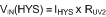
Equation 19. 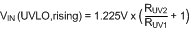
where
- IHYS = 20 μA
Setting UVLO hysteresis of 2.5 V and UVLO rising threshold of 12 V results in RUV1 = 14.53 kΩ and
RUV2 = 125 kΩ. Selecting standard values of RUV1 = R7 = 14 kΩ and RUV2 = R5 = 127 kΩ results in UVLO thresholds and hysteresis of 12.5 V to 2.5 V, respectively.