SNVS953G December 2012 – May 2021 LM25018
PRODUCTION DATA
- 1 Features
- 2 Applications
- 3 Description
- 4 Revision History
- 5 Pin Configuration and Functions
- 6 Specifications
-
7 Detailed Description
- 7.1 Overview
- 7.2 Functional Block Diagram
- 7.3
Feature Description
- 7.3.1 Control Overview
- 7.3.2 VCC Regulator
- 7.3.3 Regulation Comparator
- 7.3.4 Overvoltage Comparator
- 7.3.5 On-Time Generator
- 7.3.6 Current Limit
- 7.3.7 N-Channel Buck Switch and Driver
- 7.3.8 Synchronous Rectifier
- 7.3.9 Undervoltage Detector
- 7.3.10 Thermal Protection
- 7.3.11 Ripple Configuration
- 7.3.12 Soft Start
- 7.4 Device Functional Modes
-
8 Application and Implementation
- 8.1 Application Information
- 8.2
Typical Applications
- 8.2.1 Application Circuit: 12.5-V to 48-V Input and 10-V, 325-mA Output Buck Converter
- 8.2.2 Application Curves
- 8.2.3
Typical Isolated DC-DC Converter Using LM25018
- 8.2.3.1 Design Requirements
- 8.2.3.2
Detailed Design Procedure
- 8.2.3.2.1 Transformer Turns Ratio
- 8.2.3.2.2 Total IOUT
- 8.2.3.2.3 RFB1, RFB2
- 8.2.3.2.4 Frequency Selection
- 8.2.3.2.5 Transformer Selection
- 8.2.3.2.6 Primary Output Capacitor
- 8.2.3.2.7 Secondary Output Capacitor
- 8.2.3.2.8 Type III Feedback Ripple Circuit
- 8.2.3.2.9 Secondary Diode
- 8.2.3.2.10 VCC and Bootstrap Capacitor
- 8.2.3.2.11 Input Capacitor
- 8.2.3.2.12 UVLO Resistors
- 8.2.3.2.13 VCC Diode
- 8.2.3.3 Application Curves
- 9 Power Supply Recommendations
- 10Layout
- 11Device and Documentation Support
- 12Mechanical, Packaging, and Orderable Information
Package Options
Mechanical Data (Package|Pins)
Thermal pad, mechanical data (Package|Pins)
- DDA|8
Orderable Information
7.3.12 Soft Start
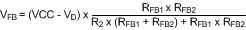
A soft-start feature can be implemented with the LM25018 using an external circuit. As shown in Figure 7-3, the soft-start circuit consists of one capacitor, C1, two resistors, R1 and R2, and a diode, D. During the initial start-up, the VCC voltage is established prior to the VOUT voltage. Capacitor C1 is discharged and D is thereby forward biased. The FB voltage is pulled up above the reference voltage (1.225 V) and switching is thereby disabled. As capacitor C1 charges, the voltage at node B gradually decreases and switching commences. VOUT gradually rises to maintain the FB voltage at the reference voltage. Once the voltage at node B is less than a diode drop above the FB voltage, the soft-start sequence is finished and D is reverse biased.
During the initial part of the start-up, the FB voltage can be approximated as shown in Equation 8.
C1 is charged after the first start-up. Diode D1 is optional and can be added to discharge C1 and initialize the soft-start sequence when the input voltage experiences a momentary drop.
To achieve the desired soft start, the following design guidance is recommended:
- R2 is selected so that VFB is higher than 1.225 V for a VCC of 4.5 V, but is lower than 5 V when VCC is 8.55 V. If an external VCC is used, VFB must not exceed 5 V at maximum VCC.
- C1 is selected to achieve the desired start-up time which can be determined from Equation 9.
Equation 9.
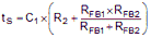
- R1 is used to maintain the node B voltage at zero after the soft start is finished. A value larger than the feedback resistor divider is preferred. Note that the effect of resistor R1 is ignored in Equation 9.
With component values from the applications schematic shown in Figure 8-1, selecting C1 = 1 µF, R2 = 1 kΩ, and R1 = 30 kΩ results in a soft-start time of about 2 ms.
 Figure 7-3 Soft-Start Circuit