SNVS726F July 2011 – March 2018 LM25118
PRODUCTION DATA.
- 1 Features
- 2 Applications
- 3 Description
- 4 Revision History
- 5 Pin Configuration and Functions
- 6 Specifications
- 7 Detailed Description
-
8 Application and Implementation
- 8.1 Application Information
- 8.2
Typical Application
- 8.2.1 Design Requirements
- 8.2.2
Detailed Design Procedure
- 8.2.2.1 Custom Design With WEBENCH® Tools
- 8.2.2.2 R7 = RT
- 8.2.2.3 Inductor Selection – L1
- 8.2.2.4 R13 = RSENSE
- 8.2.2.5 C15 = CRAMP
- 8.2.2.6 Inductor Current Limit Calculation
- 8.2.2.7 C9 - C12 = Output Capacitors
- 8.2.2.8 D1
- 8.2.2.9 D4
- 8.2.2.10 C1 – C5 = Input Capacitors
- 8.2.2.11 C20
- 8.2.2.12 C8
- 8.2.2.13 C16 = CSS
- 8.2.2.14 R8, R9
- 8.2.2.15 R1, R3, C21
- 8.2.2.16 R2
- 8.2.2.17 Snubber
- 8.2.2.18 Error Amplifier Configuration
- 8.2.3 Application Curves
- 9 Power Supply Recommendations
- 10Layout
- 11Device and Documentation Support
- 12Mechanical, Packaging, and Orderable Information
Package Options
Mechanical Data (Package|Pins)
- PWP|20
Thermal pad, mechanical data (Package|Pins)
- PWP|20
Orderable Information
7.3.3 Error Amplifier and PWM Comparator
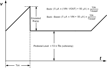
The internal high gain error amplifier generates an error signal proportional to the difference between the regulated output voltage and an internal precision reference (1.23 V). The output of the error amplifier is connected to the COMP pin. Loop compensation components, typically a type II network shown in Figure 18 are connected between the COMP and FB pins. This network creates a low-frequency pole, a zero, and a noise reducing high-frequency pole. The PWM comparator compares the emulated current sense signal from the RAMP generator to the error amplifier output voltage at the COMP pin. The same error amplifier is used for operation in buck and buck-boost mode.
 Figure 13. Composition of Emulated Current Signal