SNVSC11 May 2022 LM25143-Q1
PRODUCTION DATA
- 1 Features
- 2 Applications
- 3 Description
- 4 Revision History
- 5 Description (continued)
- 6 Device Comparison Table
- 7 Pin Configuration and Functions
- 8 Specifications
-
9 Detailed Description
- 9.1 Overview
- 9.2 Functional Block Diagram
- 9.3
Feature Description
- 9.3.1 Input Voltage Range (VIN)
- 9.3.2 High-Voltage Bias Supply Regulator (VCC, VCCX, VDDA)
- 9.3.3 Enable (EN1, EN2)
- 9.3.4 Power-Good Monitor (PG1, PG2)
- 9.3.5 Switching Frequency (RT)
- 9.3.6 Clock Synchronization (DEMB)
- 9.3.7 Synchronization Out (SYNCOUT)
- 9.3.8 Spread Spectrum Frequency Modulation (DITH)
- 9.3.9 Configurable Soft Start (SS1, SS2)
- 9.3.10 Output Voltage Setpoint (FB1, FB2)
- 9.3.11 Minimum Controllable On Time
- 9.3.12 Error Amplifier and PWM Comparator (FB1, FB2, COMP1, COMP2)
- 9.3.13 Slope Compensation
- 9.3.14 Inductor Current Sense (CS1, VOUT1, CS2, VOUT2)
- 9.3.15 Hiccup Mode Current Limiting (RES)
- 9.3.16 High-Side and Low-Side Gate Drivers (HO1, HO2, LO1, LO2, HOL1, HOL2, LOL1, and LOL2)
- 9.3.17 Output Configurations (MODE, FB2)
- 9.4 Device Functional Modes
-
10Application and Implementation
- 10.1 Application Information
- 10.2
Typical Applications
- 10.2.1 Design 1 – 5-V and 3.3-V Dual-Output Buck Regulator for Automotive Applications
- 10.2.2 Design 2 – Two-Phase, 15-A, 2.1-MHz Single-Output Buck Regulator for Automotive ADAS Applications
- 10.2.3 Design 3 – Two-Phase, 50-A, 300-kHz Single-Output Buck Regulator for High-Voltage Automotive Battery Applications
- 11Power Supply Recommendations
- 12Layout
- 13Device and Documentation Support
- 14Mechanical, Packaging, and Orderable Information
Package Options
Mechanical Data (Package|Pins)
- RHA|40
Thermal pad, mechanical data (Package|Pins)
- RHA|40
Orderable Information
9.3.11 Minimum Controllable On Time
There are two limitations to the minimum output voltage adjustment range: the LM25143-Q1 voltage reference of 0.6 V and the minimum controllable switch-node pulse width, tON(min).
tON(min) effectively limits the voltage step-down conversion ratio of VOUT/VIN at a given switching frequency. For fixed-frequency PWM operation, the voltage conversion ratio must satisfy Equation 8.
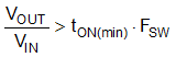
where
- tON(min) is 65 ns (typical).
- fSW is the switching frequency.
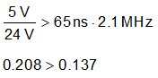
If the desired voltage conversion ratio does not meet the above condition, the LM25143-Q1 transitions from fixed switching frequency operation to a pulse-skipping mode to maintain output voltage regulation. For example, if the desired output voltage is 5 V with an input voltage is 24 V and switching frequency of 2.1 MHz, the voltage conversion ratio test in Equation 9 is satisfied.
For wide VIN applications and low output voltages, an alternative is to reduce the LM25143-Q1 switching frequency to meet the requirement of Equation 8.