SNVSC11 May 2022 LM25143-Q1
PRODUCTION DATA
- 1 Features
- 2 Applications
- 3 Description
- 4 Revision History
- 5 Description (continued)
- 6 Device Comparison Table
- 7 Pin Configuration and Functions
- 8 Specifications
-
9 Detailed Description
- 9.1 Overview
- 9.2 Functional Block Diagram
- 9.3
Feature Description
- 9.3.1 Input Voltage Range (VIN)
- 9.3.2 High-Voltage Bias Supply Regulator (VCC, VCCX, VDDA)
- 9.3.3 Enable (EN1, EN2)
- 9.3.4 Power-Good Monitor (PG1, PG2)
- 9.3.5 Switching Frequency (RT)
- 9.3.6 Clock Synchronization (DEMB)
- 9.3.7 Synchronization Out (SYNCOUT)
- 9.3.8 Spread Spectrum Frequency Modulation (DITH)
- 9.3.9 Configurable Soft Start (SS1, SS2)
- 9.3.10 Output Voltage Setpoint (FB1, FB2)
- 9.3.11 Minimum Controllable On Time
- 9.3.12 Error Amplifier and PWM Comparator (FB1, FB2, COMP1, COMP2)
- 9.3.13 Slope Compensation
- 9.3.14 Inductor Current Sense (CS1, VOUT1, CS2, VOUT2)
- 9.3.15 Hiccup Mode Current Limiting (RES)
- 9.3.16 High-Side and Low-Side Gate Drivers (HO1, HO2, LO1, LO2, HOL1, HOL2, LOL1, and LOL2)
- 9.3.17 Output Configurations (MODE, FB2)
- 9.4 Device Functional Modes
-
10Application and Implementation
- 10.1 Application Information
- 10.2
Typical Applications
- 10.2.1 Design 1 – 5-V and 3.3-V Dual-Output Buck Regulator for Automotive Applications
- 10.2.2 Design 2 – Two-Phase, 15-A, 2.1-MHz Single-Output Buck Regulator for Automotive ADAS Applications
- 10.2.3 Design 3 – Two-Phase, 50-A, 300-kHz Single-Output Buck Regulator for High-Voltage Automotive Battery Applications
- 11Power Supply Recommendations
- 12Layout
- 13Device and Documentation Support
- 14Mechanical, Packaging, and Orderable Information
Package Options
Mechanical Data (Package|Pins)
- RHA|40
Thermal pad, mechanical data (Package|Pins)
- RHA|40
Orderable Information
9.3.14.1 Shunt Current Sensing
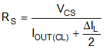
Figure 9-4 illustrates inductor current sensing using a shunt resistor. This configuration continuously monitors the inductor current to provide accurate overcurrent protection across the operating temperature range. For optimal current sense accuracy and overcurrent protection, use a low inductance ±1% tolerance shunt resistor between the inductor and the output, with a Kelvin connection to the LM25143-Q1 current sense amplifier.
If the peak differential current signal sensed from CS to VOUT exceeds the current limit threshold of 73 mV, the current limit comparator immediately terminates the applicable HO output for cycle-by-cycle current limiting. Use Equation 11 to calculate the shunt resistance.
where
- VCS is current sense threshold of 73 mV.
- IOUT(CL) is the overcurrent setpoint that is set higher than the maximum load current to avoid tripping the overcurrent comparator during load transients.
- ΔIL is the peak-to-peak inductor ripple current.
The respective SS voltage is clamped 150 mV above FB during an overcurrent condition for each channel. Sixteen overcurrent events must occur before the SS clamp is enabled. This action makes sure that SS can be pulled low during brief overcurrent events, preventing output voltage overshoot during recovery.