SNVSC05 December 2021 LM25148
PRODUCTION DATA
- 1 Features
- 2 Applications
- 3 Description
- 4 Revision History
- 5 Description (continued)
- 6 Pin Configuration and Functions
- 7 Specifications
-
8 Detailed Description
- 8.1 Overview
- 8.2 Functional Block Diagram
- 8.3
Feature Description
- 8.3.1 Input Voltage Range (VIN)
- 8.3.2 High-Voltage Bias Supply Regulator (VCC, VCCX, VDDA)
- 8.3.3 Precision Enable (EN)
- 8.3.4 Power-Good Monitor (PG)
- 8.3.5 Switching Frequency (RT)
- 8.3.6 Dual Random Spread Spectrum (DRSS)
- 8.3.7 Soft Start
- 8.3.8 Output Voltage Setpoint (FB)
- 8.3.9 Minimum Controllable On Time
- 8.3.10 Error Amplifier and PWM Comparator (FB, EXTCOMP)
- 8.3.11 Slope Compensation
- 8.3.12 Inductor Current Sense (ISNS+, VOUT)
- 8.3.13 Hiccup Mode Current Limiting
- 8.3.14 High-Side and Low-Side Gate Drivers (HO, LO)
- 8.3.15 Output Configurations (CNFG)
- 8.3.16 Single-Output Dual-Phase Operation
- 8.4 Device Functional Modes
-
9 Application and Implementation
- 9.1 Application Information
- 9.2
Typical Applications
- 9.2.1
Design 1 – High Efficiency 2.1-MHz Synchronous
Buck Regulator
- 9.2.1.1 Design Requirements
- 9.2.1.2
Detailed Design Procedure
- 9.2.1.2.1 Custom Design With WEBENCH® Tools
- 9.2.1.2.2 Custom Design With Excel Quickstart Tool
- 9.2.1.2.3 Buck Inductor
- 9.2.1.2.4 Current-Sense Resistance
- 9.2.1.2.5 Output Capacitors
- 9.2.1.2.6 Input Capacitors
- 9.2.1.2.7 Frequency Set Resistor
- 9.2.1.2.8 Feedback Resistors
- 9.2.1.2.9 Compensation Components
- 9.2.1.3 Application Curves
- 9.2.2 Design 2 – High Efficiency 440-kHz Synchronous Buck Regulator
- 9.2.3 Design 3 – Dual-Phase 400-kHz 20-A Synchronous Buck Regulator
- 9.2.1
Design 1 – High Efficiency 2.1-MHz Synchronous
Buck Regulator
- 10Power Supply Recommendations
- 11Layout
- 12Device and Documentation Support
- 13Mechanical, Packaging, and Orderable Information
Package Options
Mechanical Data (Package|Pins)
- RGY|24
Thermal pad, mechanical data (Package|Pins)
- RGY|24
Orderable Information
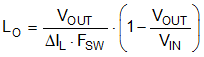
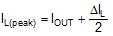
9.1.1.1 Buck Inductor
For most applications, choose a buck inductance such that the inductor ripple current, ΔIL, is between 30% to 50% of the maximum DC output current at nominal input voltage. Choose the inductance using Equation 12 based on a peak inductor current given by Equation 13.
Check the inductor data sheet to make sure that the saturation current of the inductor is well above the peak inductor current of a particular design. Ferrite designs have very low core loss and are preferred at high switching frequencies, so design goals can then concentrate on copper loss and preventing saturation. Low inductor core loss is evidenced by reduced no-load input current and higher light-load efficiency. However, ferrite core materials exhibit a hard saturation characteristic and the inductance collapses abruptly when the saturation current is exceeded. This results in an abrupt increase in inductor ripple current and higher output voltage ripple, not to mention reduced efficiency and compromised reliability. Note that the saturation current of an inductor generally decreases as its core temperature increases. Of course, accurate overcurrent protection is key to avoiding inductor saturation.