SNVSC05 December 2021 LM25148
PRODUCTION DATA
- 1 Features
- 2 Applications
- 3 Description
- 4 Revision History
- 5 Description (continued)
- 6 Pin Configuration and Functions
- 7 Specifications
-
8 Detailed Description
- 8.1 Overview
- 8.2 Functional Block Diagram
- 8.3
Feature Description
- 8.3.1 Input Voltage Range (VIN)
- 8.3.2 High-Voltage Bias Supply Regulator (VCC, VCCX, VDDA)
- 8.3.3 Precision Enable (EN)
- 8.3.4 Power-Good Monitor (PG)
- 8.3.5 Switching Frequency (RT)
- 8.3.6 Dual Random Spread Spectrum (DRSS)
- 8.3.7 Soft Start
- 8.3.8 Output Voltage Setpoint (FB)
- 8.3.9 Minimum Controllable On Time
- 8.3.10 Error Amplifier and PWM Comparator (FB, EXTCOMP)
- 8.3.11 Slope Compensation
- 8.3.12 Inductor Current Sense (ISNS+, VOUT)
- 8.3.13 Hiccup Mode Current Limiting
- 8.3.14 High-Side and Low-Side Gate Drivers (HO, LO)
- 8.3.15 Output Configurations (CNFG)
- 8.3.16 Single-Output Dual-Phase Operation
- 8.4 Device Functional Modes
-
9 Application and Implementation
- 9.1 Application Information
- 9.2
Typical Applications
- 9.2.1
Design 1 – High Efficiency 2.1-MHz Synchronous
Buck Regulator
- 9.2.1.1 Design Requirements
- 9.2.1.2
Detailed Design Procedure
- 9.2.1.2.1 Custom Design With WEBENCH® Tools
- 9.2.1.2.2 Custom Design With Excel Quickstart Tool
- 9.2.1.2.3 Buck Inductor
- 9.2.1.2.4 Current-Sense Resistance
- 9.2.1.2.5 Output Capacitors
- 9.2.1.2.6 Input Capacitors
- 9.2.1.2.7 Frequency Set Resistor
- 9.2.1.2.8 Feedback Resistors
- 9.2.1.2.9 Compensation Components
- 9.2.1.3 Application Curves
- 9.2.2 Design 2 – High Efficiency 440-kHz Synchronous Buck Regulator
- 9.2.3 Design 3 – Dual-Phase 400-kHz 20-A Synchronous Buck Regulator
- 9.2.1
Design 1 – High Efficiency 2.1-MHz Synchronous
Buck Regulator
- 10Power Supply Recommendations
- 11Layout
- 12Device and Documentation Support
- 13Mechanical, Packaging, and Orderable Information
Package Options
Mechanical Data (Package|Pins)
- RGY|24
Thermal pad, mechanical data (Package|Pins)
- RGY|24
Orderable Information
8.3.12.2 Inductor DCR Current Sensing
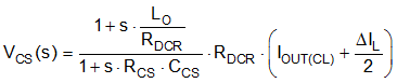
For high-power applications that do not require accurate current-limit protection, inductor DCR current sensing is preferable. This technique provides lossless and continuous monitoring of the inductor current using an RC sense network in parallel with the inductor. Select an inductor with a low DCR tolerance to achieve a typical current limit accuracy within the range of 10% to 15% at room temperature. Components RCS and CCS in Figure 8-4 create a low-pass filter across the inductor to enable differential sensing of the voltage across the inductor DCR.
 Figure 8-4 Inductor DCR Current Sensing
Implementation
Figure 8-4 Inductor DCR Current Sensing
ImplementationThe voltage drop across the sense capacitor in the s-domain is given by Equation 10. When the RCSCCS time constant is equal to LO/RDCR, the voltage developed across the sense capacitor, CCS, is a replica of the inductor DCR voltage and accurate current sensing is achieved. If the RCSCCS time constant is not equal to the LO/RDCR time constant, there is a sensing error as follows:
- RCSCCS > LO/RDCR → the DC level is correct, but the AC amplitude is attenuated.
- RCSCCS < LO/RDCR → the DC level is correct, but the AC amplitude is amplified.
Choose the CCS capacitance greater than or equal to 0.1 μF to maintain a low-impedance sensing network, thus reducing the susceptibility of noise pickup from the switch node. Carefully observe Section 11.1 to make sure that noise and DC errors do not corrupt the current sense signals applied between the ISNS+ and VOUT pins.