SNVSBV5B December 2020 – December 2021 LM25149
PRODUCTION DATA
- 1 Features
- 2 Applications
- 3 Description
- 4 Revision History
- 5 Description (continued)
- 6 Pin Configuration and Functions
- 7 Specifications
-
8 Detailed Description
- 8.1 Overview
- 8.2 Functional Block Diagram
- 8.3
Feature Description
- 8.3.1 Input Voltage Range (VIN)
- 8.3.2 High-Voltage Bias Supply Regulator (VCC, VCCX, VDDA)
- 8.3.3 Precision Enable (EN)
- 8.3.4 Power-Good Monitor (PG)
- 8.3.5 Switching Frequency (RT)
- 8.3.6 Active EMI Filter
- 8.3.7 Dual Random Spread Spectrum (DRSS)
- 8.3.8 Soft Start
- 8.3.9 Output Voltage Setpoint (FB)
- 8.3.10 Minimum Controllable On Time
- 8.3.11 Error Amplifier and PWM Comparator (FB, EXTCOMP)
- 8.3.12 Slope Compensation
- 8.3.13 Inductor Current Sense (ISNS+, VOUT)
- 8.3.14 Hiccup Mode Current Limiting
- 8.3.15 High-Side and Low-Side Gate Drivers (HO, LO)
- 8.3.16 Output Configurations (CNFG)
- 8.3.17 Single-Output Dual-Phase Operation
- 8.4 Device Functional Modes
-
9 Application and Implementation
- 9.1 Application Information
- 9.2
Typical Applications
- 9.2.1
Design 1 – High Efficiency 2.1-MHz Synchronous
Buck Regulator
- 9.2.1.1 Design Requirements
- 9.2.1.2
Detailed Design Procedure
- 9.2.1.2.1 Custom Design With WEBENCH® Tools
- 9.2.1.2.2 Custom Design With Excel Quickstart Tool
- 9.2.1.2.3 Buck Inductor
- 9.2.1.2.4 Current-Sense Resistance
- 9.2.1.2.5 Output Capacitors
- 9.2.1.2.6 Input Capacitors
- 9.2.1.2.7 Frequency Set Resistor
- 9.2.1.2.8 Feedback Resistors
- 9.2.1.2.9 Compensation Components
- 9.2.1.2.10 Active EMI Components
- 9.2.1.3 Application Curves
- 9.2.2 Design 2 – High Efficiency 440-kHz Synchronous Buck Regulator
- 9.2.3 Design 3 – Dual-Phase 400-kHz 20-A Synchronous Buck Regulator
- 9.2.1
Design 1 – High Efficiency 2.1-MHz Synchronous
Buck Regulator
- 10Power Supply Recommendations
- 11Layout
- 12Device and Documentation Support
- 13Mechanical, Packaging, and Orderable Information
Package Options
Mechanical Data (Package|Pins)
- RGY|24
Thermal pad, mechanical data (Package|Pins)
- RGY|24
Orderable Information
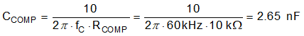
9.2.1.2.9 Compensation Components
Choose compensation components for a stable control loop using the procedure outlined as follows:
- Based on a specified loop gain crossover
frequency, fC, of 60 kHz, use Equation 48 to calculate RCOMP, assuming an effective output capacitance of
100 µF. Choose a standard value for RCOMP of 10 kΩ. Equation 45.

- To provide adequate phase boost at crossover
while also allowing a fast settling time during a load or line transient, select
CCOMP to place a zero at the higher of (1) one tenth of the
crossover frequency, or (2) the load pole. Choose a standard value for
CCOMP of 2.7 nF. Equation 46.
Such a low capacitance value also helps to avoid output voltage overshoot when recovering from dropout (when the input voltage is less than the output voltage setpoint and VCOMP is railed high).
- Calculate CHF to create a pole at the
ESR zero and to attenuate high-frequency noise at COMP. CBW is the
bandwidth-limiting capacitance of the error amplifier. CHF may not be
significant enough to be necessary in some designs, like this one.
CHF can be unpopulated, or used with a small 22 pF for more noise
filtering.Equation 47.

Note:
Set a fast loop with high RCOMP and low CCOMP values to improve the response when recovering from operation in dropout.
| For technical solutions, industry trends, and insights for designing and managing power supplies, please refer to TI's technical articles. |