SNVSBV5B December 2020 – December 2021 LM25149
PRODUCTION DATA
- 1 Features
- 2 Applications
- 3 Description
- 4 Revision History
- 5 Description (continued)
- 6 Pin Configuration and Functions
- 7 Specifications
-
8 Detailed Description
- 8.1 Overview
- 8.2 Functional Block Diagram
- 8.3
Feature Description
- 8.3.1 Input Voltage Range (VIN)
- 8.3.2 High-Voltage Bias Supply Regulator (VCC, VCCX, VDDA)
- 8.3.3 Precision Enable (EN)
- 8.3.4 Power-Good Monitor (PG)
- 8.3.5 Switching Frequency (RT)
- 8.3.6 Active EMI Filter
- 8.3.7 Dual Random Spread Spectrum (DRSS)
- 8.3.8 Soft Start
- 8.3.9 Output Voltage Setpoint (FB)
- 8.3.10 Minimum Controllable On Time
- 8.3.11 Error Amplifier and PWM Comparator (FB, EXTCOMP)
- 8.3.12 Slope Compensation
- 8.3.13 Inductor Current Sense (ISNS+, VOUT)
- 8.3.14 Hiccup Mode Current Limiting
- 8.3.15 High-Side and Low-Side Gate Drivers (HO, LO)
- 8.3.16 Output Configurations (CNFG)
- 8.3.17 Single-Output Dual-Phase Operation
- 8.4 Device Functional Modes
-
9 Application and Implementation
- 9.1 Application Information
- 9.2
Typical Applications
- 9.2.1
Design 1 – High Efficiency 2.1-MHz Synchronous
Buck Regulator
- 9.2.1.1 Design Requirements
- 9.2.1.2
Detailed Design Procedure
- 9.2.1.2.1 Custom Design With WEBENCH® Tools
- 9.2.1.2.2 Custom Design With Excel Quickstart Tool
- 9.2.1.2.3 Buck Inductor
- 9.2.1.2.4 Current-Sense Resistance
- 9.2.1.2.5 Output Capacitors
- 9.2.1.2.6 Input Capacitors
- 9.2.1.2.7 Frequency Set Resistor
- 9.2.1.2.8 Feedback Resistors
- 9.2.1.2.9 Compensation Components
- 9.2.1.2.10 Active EMI Components
- 9.2.1.3 Application Curves
- 9.2.2 Design 2 – High Efficiency 440-kHz Synchronous Buck Regulator
- 9.2.3 Design 3 – Dual-Phase 400-kHz 20-A Synchronous Buck Regulator
- 9.2.1
Design 1 – High Efficiency 2.1-MHz Synchronous
Buck Regulator
- 10Power Supply Recommendations
- 11Layout
- 12Device and Documentation Support
- 13Mechanical, Packaging, and Orderable Information
Package Options
Mechanical Data (Package|Pins)
- RGY|24
Thermal pad, mechanical data (Package|Pins)
- RGY|24
Orderable Information
9.2.1.2.4 Current-Sense Resistance
- Calculate the current-sense resistance based on a
maximum peak current capability of at least 25% higher than the peak inductor
current at full load to provide sufficient margin during start-up and load-on
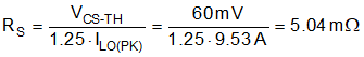
transients. Calculate the current sense resistances using Equation 36. Equation 36.
where
- VCS-TH is the 60-mV current limit threshold.
- Select a standard resistance value of 5 mΩ for the shunt. An 0508 footprint component with wide aspect ratio termination design provides 1-W power rating, low parasitic series inductance, and compact PCB layout. Carefully adhere to the layout guidelines in Section 11.1 to make sure that noise and DC errors do not corrupt the differential current-sense voltages measured at the ISNS+ and VOUT pins.
- Place the shunt resistor close to the inductor.
- Use Kelvin-sense connections, and route the sense lines differentially from the shunt to the LM25149.
- The CS-to-output propagation delay (related to
the current limit comparator, internal logic, and power MOSFET gate drivers)
causes the peak current to increase above the calculated current limit
threshold. For a total propagation delay tDELAY-ISNS+ of 40 ns, use
Equation 37 to calculate the worst-case peak inductor current with the output shorted.
Equation 37.

- Based on this result, select an inductor with saturation current greater than 16 A across the full operating temperature range.