SNVSB19 December 2017 LM25574-Q1
PRODUCTION DATA.
- 1 Features
- 2 Applications
- 3 Description
- 4 Revision History
- 5 Pin Configuration and Functions
- 6 Specifications
- 7 Detailed Description
- 8 Application and Implementation
- 9 Layout
- 10Device and Documentation Support
- 11Mechanical, Packaging, and Orderable Information
Package Options
Mechanical Data (Package|Pins)
- PW|16
Thermal pad, mechanical data (Package|Pins)
Orderable Information
1 Features
- Qualified for Automotive Applications
- AEC-Q100 Qualified With the Following Results:
- Device Temperature Grade 1: –40°C to +125°C Ambient Operating Temperature
- Integrated 42-V, 750-mΩ N-Channel MOSFET
- Ultra-Wide Input Voltage From 6 V to 42 V
- Adjustable Output Voltage as Low as 1.225 V
- 1.5% Feedback Reference Accuracy
- Operating Frequency Adjustable Between 50 kHz and 1 MHz With Single Resistor
- Master or Slave Frequency Synchronization
- Adjustable Soft-Start
- Emulated Current Mode Control Architecture
- Wide Bandwidth Error Amplifier
- Built-In Protection
- TSSOP-16 Package
- Create a Custom Design Using the LM25574-Q1 With the WEBENCH® Power Designer
2 Applications
- Industrial
3 Description
The LM25574-Q1 is an easy to use buck regulator which allows design engineers to design and optimize a robust power supply using a minimum set of components. Operating with an input voltage range of 6 V to 42 V, the LM25574-Q1 delivers 0.5-A of continuous output current with an integrated 750-mΩ N-Channel MOSFET. The regulator utilizes an Emulated Current Mode architecture which provides inherent line regulation, tight load transient response, and ease of loop compensation without the usual limitation of low-duty cycles associated with current mode regulators. The operating frequency is adjustable from 50 kHz to 1-MHz to allow optimization of size and efficiency. To reduce EMI, a frequency synchronization pin allows multiple IC’s from the LM(2)557x family to self-synchronize or to synchronize to an external clock. The LM25574-Q1 guarantees robustness with cycle-by-cycle current limit, short-circuit protection, thermal shut-down, and remote shut-down. The device is available in a TSSOP-16 package.
Device Information(1)
| PART NUMBER | PACKAGE | BODY SIZE (NOM) |
|---|---|---|
| LM25574-Q1 | TSSOP (16) | 5.00 mm × 4.40 mm |
- For all available packages, see the orderable addendum at the end of the data sheet.
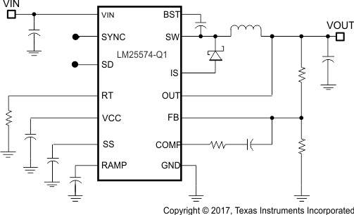
Simplified Application Schematic
