SNVS107G June   1999  – March 2023 LM2576 , LM2576HV

PRODUCTION DATA  

  1. Features
  2. Applications
  3. Description
  4. Revision History
  5. Pin Configuration and Functions
  6. Specifications
    1. 6.1  Absolute Maximum Ratings
    2. 6.2  ESD Ratings
    3. 6.3  Recommended Operating Conditions
    4. 6.4  Thermal Information
    5. 6.5  Electrical Characteristics: 3.3 V
    6. 6.6  Electrical Characteristics: 5 V
    7. 6.7  Electrical Characteristics: 12 V
    8. 6.8  Electrical Characteristics: 15 V
    9. 6.9  Electrical Characteristics: Adjustable Output Voltage
    10. 6.10 Electrical Characteristics: All Output Voltage Versions
    11. 6.11 Typical Characteristics
  7. Detailed Description
    1. 7.1 Overview
    2. 7.2 Functional Block Diagram
    3. 7.3 Feature Description
      1. 7.3.1 Undervoltage Lockout
      2. 7.3.2 Delayed Start-Up
      3. 7.3.3 Adjustable Output, Low-Ripple Power Supply
    4. 7.4 Device Functional Modes
      1. 7.4.1 Shutdown Mode
      2. 7.4.2 Active Mode
      3. 7.4.3 Current Limit
  8. Application and Implementation
    1. 8.1 Application Information
      1. 8.1.1  Input Capacitor (CIN)
      2. 8.1.2  Inductor Selection
      3. 8.1.3  Inductor Ripple Current
      4. 8.1.4  Output Capacitor
      5. 8.1.5  Catch Diode
      6. 8.1.6  Output Voltage Ripple and Transients
      7. 8.1.7  Feedback Connection
      8. 8.1.8  ON /OFF INPUT
      9. 8.1.9  Inverting Regulator
      10. 8.1.10 Negative Boost Regulator
    2. 8.2 Typical Applications
      1. 8.2.1 Fixed Output Voltage Version
        1. 8.2.1.1 Design Requirements
        2. 8.2.1.2 Detailed Design Procedure
          1. 8.2.1.2.1 Custom Design with WEBENCH® Tools
          2. 8.2.1.2.2 Inductor Selection (L1)
          3. 8.2.1.2.3 Output Capacitor Selection (COUT)
          4. 8.2.1.2.4 Catch Diode Selection (D1)
          5. 8.2.1.2.5 Input Capacitor (CIN)
        3. 8.2.1.3 Application Curves
      2. 8.2.2 Adjusted Output Voltage Version
        1. 8.2.2.1 Design Requirements
        2. 8.2.2.2 Detailed Design Procedure
          1. 8.2.2.2.1 Programming Output Voltage
          2. 8.2.2.2.2 Inductor Selection (L1)
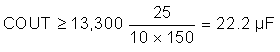
          3. 8.2.2.2.3 Output Capacitor Selection (COUT)
          4. 8.2.2.2.4 Catch Diode Selection (D1)
          5. 8.2.2.2.5 Input Capacitor (CIN)
    3. 8.3 Power Supply Recommendations
    4. 8.4 Layout
      1. 8.4.1 Layout Guidelines
      2. 8.4.2 Layout Example
      3. 8.4.3 Grounding
      4. 8.4.4 Heat Sink and Thermal Considerations
  9. Device and Documentation Support
    1. 9.1 Device Support
      1. 9.1.1 Device Nomenclature
        1. 9.1.1.1 Definition of Terms
      2. 9.1.2 Development Support
        1. 9.1.2.1 Custom Design with WEBENCH® Tools
    2. 9.2 Documentation Support
      1. 9.2.1 Related Documentation
    3. 9.3 Support Resources
    4. 9.4 Receiving Notification of Documentation Updates
    5. 9.5 Trademarks
    6. 9.6 Electrostatic Discharge Caution
    7. 9.7 Glossary
  10. 10Mechanical, Packaging, and Orderable Information

Package Options

Refer to the PDF data sheet for device specific package drawings

Mechanical Data (Package|Pins)
  • NDH|5
  • NEB|5
  • KTT|5
  • KC|5
Thermal pad, mechanical data (Package|Pins)
Orderable Information
Output Capacitor Selection (COUT)
  1. The value of the output capacitor together with the inductor defines the dominate pole-pair of the switching regulator loop. For stable operation, the capacitor must satisfy Equation 11:
    GUID-C5366972-AC5F-44C0-85E0-B812DE6560D4-low.gif

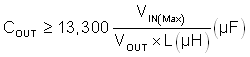
    Equation 11 yields capacitor values between 10 μF and 2200 μF that satisfies the loop requirements for stable operation. But to achieve an acceptable output ripple voltage, (approximately 1% of the output voltage) and transient response, the output capacitor can need to be several times larger than Equation 11 yields.

    GUID-66104D4C-0667-448C-B602-EE84BFD5ED63-low.gif

    However, for acceptable output ripple voltage select

    COUT ≥ 680 μF

    COUT = 680-μF electrolytic capacitor

  2. The capacitor voltage rating must be at last 1.5 times greater than the output voltage. For a 10-V regulator, TI recommends a rating of at least 15 V or more. Higher voltage electrolytic capacitors generally have lower ESR numbers, and for this reason it can be necessary to select a capacitor rate for a higher voltage than can normally be needed.