SNVS115E April 2000 – June 2019 LM2587
PRODUCTION DATA.
- 1 Features
- 2 Typical Applications
- 3 Description
- 4 Revision History
- 5 Pin Configurations
-
6 Specifications
- 6.1 Absolute Maximum Ratings
- 6.2 ESDRatings
- 6.3 Recommended Operating Ratings
- 6.4 Thermal Information
- 6.5 Electrical Characteristics: 3.3 V
- 6.6 Electrical Characteristics: 5 V
- 6.7 Electrical Characteristics: 12 V
- 6.8 Electrical Characteristics: Adjustable
- 6.9 Electrical Characteristics: All Output Voltage Versions
- 6.10 Typical Characteristics
- 7 Detailed Description
- 8 Application And Implementation
- 9 Layout
- 10Device and Documentation Support
- 11Mechanical, Packaging, and Orderable Information
Package Options
Mechanical Data (Package|Pins)
Thermal pad, mechanical data (Package|Pins)
- KTT|5
Orderable Information
9.3 Heat Sink/Thermal Considerations
In many cases, no heat sink is required to keep the LM2587 junction temperature within the allowed operating range. For each application, to determine whether or not a heat sink will be required, the following must be identified:
1) Maximum ambient temperature (in the application).
2) Maximum regulator power dissipation (in the application).
3) Maximum allowed junction temperature (125°C for the LM2587). For a safe, conservative design, a temperature approximately 15°C cooler than the maximum junction temperature should be selected (110°C).
4) LM2587 package thermal resistances θJA and θJC (given in the Electrical Characteristics).
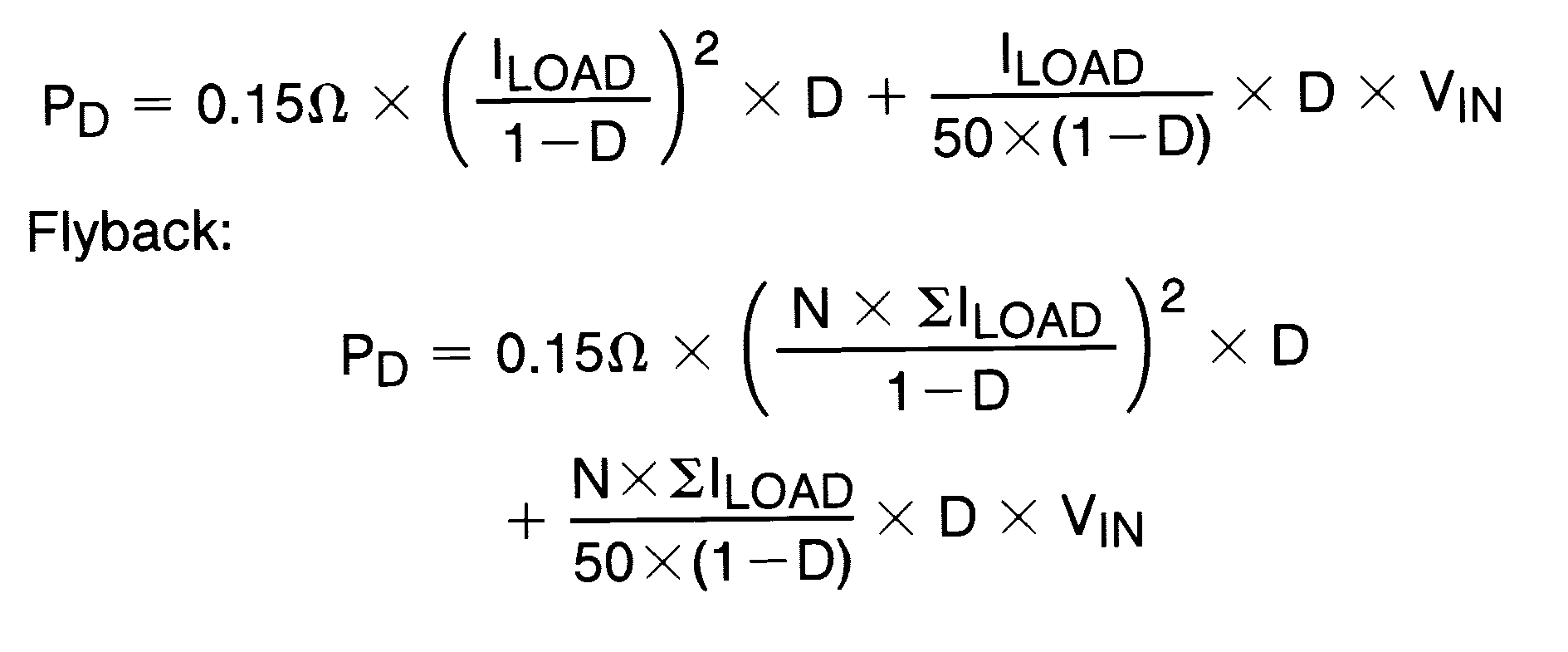
Total power dissipated (PD) by the LM2587 can be estimated as follows:
Boost:

VIN is the minimum input voltage, VOUT is the output voltage, N is the transformer turns ratio, D is the duty cycle, and ILOAD is the maximum load current (and ∑ILOAD is the sum of the maximum load currents for multiple-output flyback regulators). The duty cycle is given by:
Boost:

where
- VF is the forward biased voltage of the diode and is typically 0.5V for Schottky diodes and 0.8V for fast recovery diodes.
- VSAT is the switch saturation voltage and can be found in the Characteristic Curves.
When no heat sink is used, the junction temperature rise is:
Adding the junction temperature rise to the maximum ambient temperature gives the actual operating junction temperature:
If the operating junction temperature exceeds the maximum junction temperatue in item 3 above, then a heat sink is required. When using a heat sink, the junction temperature rise can be determined by the following:
Again, the operating junction temperature will be:
As before, if the maximum junction temperature is exceeded, a larger heat sink is required (one that has a lower thermal resistance).
Included in the Switchers Made Simple design software is a more precise (non-linear) thermal model that can be used to determine junction temperature with different input-output parameters or different component values. It can also calculate the heat sink thermal resistance required to maintain the regulator junction temperature below the maximum operating temperature.
To further simplify the flyback regulator design procedure, TI is making available computer design software. Switchers Made Simple software is available on a (3½″) diskette for IBM compatible computers from a TI sales office in your area or the TI WEBENCH Design Center team.
http://www.ti.com/ww/en/analog/webench/index.shtml?DCMP=hpa_sva_webench&HQS=webench-bb