SNVS084C December 2001 – July 2016 LM2590HV
PRODUCTION DATA.
- 1 Features
- 2 Applications
- 3 Description
- 4 Revision History
- 5 Pin Configuration and Functions
-
6 Specifications
- 6.1 Absolute Maximum Ratings
- 6.2 ESD Ratings
- 6.3 Recommended Operating Conditions
- 6.4 Thermal Information
- 6.5 Electrical Characteristics
- 6.6 Electrical Characteristics - 3.3-V Version
- 6.7 Electrical Characteristics - 5-V Version
- 6.8 Electrical Characteristics - Adjustable Version
- 6.9 Typical Characteristics
- 7 Parameter Measurement Information
- 8 Detailed Description
- 9 Application and Implementation
- 10Power Supply Recommendations
- 11Layout
- 12Device and Documentation Support
- 13Mechanical, Packaging, and Orderable Information
Package Options
Mechanical Data (Package|Pins)
Thermal pad, mechanical data (Package|Pins)
Orderable Information
7 Parameter Measurement Information
7.1 Test Circuits

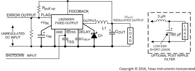
Component Values shown are for VIN = 15 V,
VOUT = 5 V, ILOAD = 1 A.
CIN — 470-µF, 50-V aluminum electrolytic Nichicon PM Series
COUT — 220-µF, 25-V aluminum electrolytic Nichcon PM Series
D1 — 2-A, 60-V Schottky Rectifier, 21DQ06 (international rectifier)
L1 — 68 µH, see Inductor Selection Procedure
Figure 24. Fixed Output Voltage Versions
VOUT = 5 V, ILOAD = 1 A.
CIN — 470-µF, 50-V aluminum electrolytic Nichicon PM Series
COUT — 220-µF, 25-V aluminum electrolytic Nichcon PM Series
D1 — 2-A, 60-V Schottky Rectifier, 21DQ06 (international rectifier)
L1 — 68 µH, see Inductor Selection Procedure

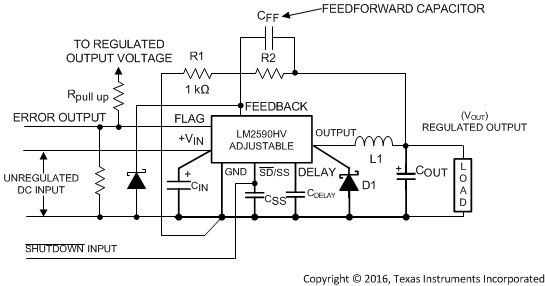
Select R1 to be approximately 1 kΩ, use a 1% resistor for best stability.
Component values shown are for VIN = 20 V,
VOUT = 10 V, ILOAD = 1 A.
CIN — 470-µF, 35-V aluminum electrolytic Nichicon PM Series
COUT — 220-µF, 35-V aluminum electrolytic Nichicon PM Series
D1 — 2-A, 60-V Schottky Rectifier, 21DQ06 (international rectifier)
L1 — 100 µH, see Inductor Selection Procedure
R1 — 1 kΩ, 1%
R2 — 7.15 k, 1%
CFF — 3.3 nF
Typical Values
CSS — 0.1 µF
CDELAY — 0.1 µF
RPULL UP — 4.7 k (use 22 k if VOUT is ≥ 45 V)
† Resistive divider is required to avoid exceeding maximum rating of 45 V, 3 mA on or into flag pin.
†† Small signal Schottky diode to prevent damage to feedback pin by negative spike when output is shorted. Required if VIN > 40 V
Figure 25. Adjustable Output Voltage Versions
Component values shown are for VIN = 20 V,
VOUT = 10 V, ILOAD = 1 A.
CIN — 470-µF, 35-V aluminum electrolytic Nichicon PM Series
COUT — 220-µF, 35-V aluminum electrolytic Nichicon PM Series
D1 — 2-A, 60-V Schottky Rectifier, 21DQ06 (international rectifier)
L1 — 100 µH, see Inductor Selection Procedure
R1 — 1 kΩ, 1%
R2 — 7.15 k, 1%
CFF — 3.3 nF
Typical Values
CSS — 0.1 µF
CDELAY — 0.1 µF
RPULL UP — 4.7 k (use 22 k if VOUT is ≥ 45 V)
† Resistive divider is required to avoid exceeding maximum rating of 45 V, 3 mA on or into flag pin.
†† Small signal Schottky diode to prevent damage to feedback pin by negative spike when output is shorted. Required if VIN > 40 V