SNVSB35B May   2018  – June 2020 LM26420-Q1

PRODUCTION DATA.  

  1. Features
  2. Applications
  3. Description
    1.     Device Images
      1.      LM26420 Dual Buck DC/DC Converter
      2.      LM26420 Efficiency (Up to 93%)
  4. Revision History
  5. Pin Configuration and Functions
    1.     Pin Functions: 16-Pin WQFN
    2.     Pin Functions 20-Pin HTSSOP
  6. Specifications
    1. 6.1 Absolute Maximum Ratings
    2. 6.2 ESD Ratings
    3. 6.3 Recommended Operating Conditions
    4. 6.4 Thermal Information
    5. 6.5 Electrical Characteristics Per Buck
    6. 6.6 Typical Characteristics
  7. Detailed Description
    1. 7.1 Overview
    2. 7.2 Functional Block Diagram
    3. 7.3 Feature Description
      1. 7.3.1 Soft Start
      2. 7.3.2 Power Good
      3. 7.3.3 Precision Enable
    4. 7.4 Device Functional Modes
      1. 7.4.1 Output Overvoltage Protection
      2. 7.4.2 Undervoltage Lockout
      3. 7.4.3 Current Limit
      4. 7.4.4 Thermal Shutdown
  8. Application and Implementation
    1. 8.1 Application Information
      1. 8.1.1 Programming Output Voltage
      2. 8.1.2 VINC Filtering Components
      3. 8.1.3 Using Precision Enable and Power Good
      4. 8.1.4 Overcurrent Protection
    2. 8.2 Typical Applications
      1. 8.2.1 2.2-MHz, 0.8-V Typical High-Efficiency Application Circuit
        1. 8.2.1.1 Design Requirements
        2. 8.2.1.2 Detailed Design Procedure
          1. 8.2.1.2.1 Custom Design With WEBENCH® Tools
          2. 8.2.1.2.2 Inductor Selection
          3. 8.2.1.2.3 Input Capacitor Selection
          4. 8.2.1.2.4 Output Capacitor
          5. 8.2.1.2.5 Calculating Efficiency and Junction Temperature
        3. 8.2.1.3 Application Curves
      2. 8.2.2 2.2-MHz, 1.8-V Typical High-Efficiency Application Circuit
        1. 8.2.2.1 Design Requirements
        2. 8.2.2.2 Detailed Design Procedure
        3. 8.2.2.3 Application Curves
      3. 8.2.3 LM26420-Q12.2-MHz, 2.5-V Typical High-Efficiency Application Circuit
        1. 8.2.3.1 Design Requirements
        2. 8.2.3.2 Detailed Design Procedure
        3. 8.2.3.3 Application Curves
  9. Power Supply Recommendations
  10. 10Layout
    1. 10.1 Layout Guidelines
    2. 10.2 Layout Example
    3. 10.3 Thermal Considerations
      1. 10.3.1 Method 1: Silicon Junction Temperature Determination
      2. 10.3.2 Thermal Shutdown Temperature Determination
  11. 11Device and Documentation Support
    1. 11.1 Device Support
      1. 11.1.1 Third-Party Products Disclaimer
      2. 11.1.2 Custom Design With WEBENCH® Tools
    2. 11.2 Documentation Support
      1. 11.2.1 Related Documentation
    3. 11.3 Receiving Notification of Documentation Updates
    4. 11.4 Support Resources
    5. 11.5 Trademarks
    6. 11.6 Electrostatic Discharge Caution
    7. 11.7 Glossary
  12. 12Mechanical, Packaging, and Orderable Information

Package Options

Mechanical Data (Package|Pins)
Thermal pad, mechanical data (Package|Pins)
Orderable Information

Inductor Selection

The duty cycle (D) can be approximated as the ratio of output voltage (VOUT) to input voltage (VIN):

Equation 5. LM26420-Q1 30069609.gif

The voltage drop across the internal NMOS (SW_BOT) and PMOS (SW_TOP) must be included to calculate a more accurate duty cycle. Calculate D by using the following formulas:

Equation 6. LM26420-Q1 30069610.gif

VSW_TOP and VSW_BOT can be approximated by:

Equation 7. VSW_TOP = IOUT × RDSON_TOP
Equation 8. VSW_BOT = IOUT × RDSON_BOT

The inductor value determines the output ripple voltage. Smaller inductor values decrease the size of the inductor, but increase the output ripple voltage. An increase in the inductor value decreases the output ripple current.

One must ensure that the minimum current limit (2.4 A) is not exceeded, so the peak current in the inductor must be calculated. The peak current (ILPK) in the inductor is calculated by:
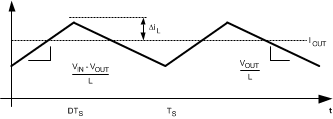
Equation 9. ILPK = IOUT + ΔiL
LM26420-Q1 30069605.gifFigure 35. Inductor Current
Equation 10. LM26420-Q1 30069613.gif

In general,

Equation 11. ΔiL = 0.1 × (IOUT) → 0.2 × (IOUT)

If ΔiL = 20% of 2 A, the peak current in the inductor is 2.4 A. The minimum ensured current limit over all operating conditions is 2.4 A. One can either reduce ΔiL, or make the engineering judgment that zero margin is safe enough. The typical current limit is 3.3 A.

The LM26420-Q1 operates at frequencies allowing the use of ceramic output capacitors without compromising transient response. Ceramic capacitors allow higher inductor ripple without significantly increasing output ripple voltage. See the Output Capacitor section for more details on calculating output voltage ripple. Now that the ripple current is determined, the inductance is calculated by:

Equation 12. LM26420-Q1 30069611.gif

where

    Equation 13. LM26420-Q1 30069612.gif

When selecting an inductor, make sure that it is capable of supporting the peak output current without saturating. Inductor saturation results in a sudden reduction in inductance and prevents the regulator from operating correctly. The peak current of the inductor is used to specify the maximum output current of the inductor and saturation is not a concern due to the exceptionally small delay of the internal current limit signal. Ferrite based inductors are preferred to minimize core losses when operating with the frequencies used by the LM26420-Q1. This presents little restriction because the variety of ferrite-based inductors is huge. Lastly, inductors with lower series resistance (RDCR) provides better operating efficiency. For recommended inductors, see Table 2.