SNVSB35B May   2018  – June 2020 LM26420-Q1

PRODUCTION DATA.  

  1. Features
  2. Applications
  3. Description
    1.     Device Images
      1.      LM26420 Dual Buck DC/DC Converter
      2.      LM26420 Efficiency (Up to 93%)
  4. Revision History
  5. Pin Configuration and Functions
    1.     Pin Functions: 16-Pin WQFN
    2.     Pin Functions 20-Pin HTSSOP
  6. Specifications
    1. 6.1 Absolute Maximum Ratings
    2. 6.2 ESD Ratings
    3. 6.3 Recommended Operating Conditions
    4. 6.4 Thermal Information
    5. 6.5 Electrical Characteristics Per Buck
    6. 6.6 Typical Characteristics
  7. Detailed Description
    1. 7.1 Overview
    2. 7.2 Functional Block Diagram
    3. 7.3 Feature Description
      1. 7.3.1 Soft Start
      2. 7.3.2 Power Good
      3. 7.3.3 Precision Enable
    4. 7.4 Device Functional Modes
      1. 7.4.1 Output Overvoltage Protection
      2. 7.4.2 Undervoltage Lockout
      3. 7.4.3 Current Limit
      4. 7.4.4 Thermal Shutdown
  8. Application and Implementation
    1. 8.1 Application Information
      1. 8.1.1 Programming Output Voltage
      2. 8.1.2 VINC Filtering Components
      3. 8.1.3 Using Precision Enable and Power Good
      4. 8.1.4 Overcurrent Protection
    2. 8.2 Typical Applications
      1. 8.2.1 2.2-MHz, 0.8-V Typical High-Efficiency Application Circuit
        1. 8.2.1.1 Design Requirements
        2. 8.2.1.2 Detailed Design Procedure
          1. 8.2.1.2.1 Custom Design With WEBENCH® Tools
          2. 8.2.1.2.2 Inductor Selection
          3. 8.2.1.2.3 Input Capacitor Selection
          4. 8.2.1.2.4 Output Capacitor
          5. 8.2.1.2.5 Calculating Efficiency and Junction Temperature
        3. 8.2.1.3 Application Curves
      2. 8.2.2 2.2-MHz, 1.8-V Typical High-Efficiency Application Circuit
        1. 8.2.2.1 Design Requirements
        2. 8.2.2.2 Detailed Design Procedure
        3. 8.2.2.3 Application Curves
      3. 8.2.3 LM26420-Q12.2-MHz, 2.5-V Typical High-Efficiency Application Circuit
        1. 8.2.3.1 Design Requirements
        2. 8.2.3.2 Detailed Design Procedure
        3. 8.2.3.3 Application Curves
  9. Power Supply Recommendations
  10. 10Layout
    1. 10.1 Layout Guidelines
    2. 10.2 Layout Example
    3. 10.3 Thermal Considerations
      1. 10.3.1 Method 1: Silicon Junction Temperature Determination
      2. 10.3.2 Thermal Shutdown Temperature Determination
  11. 11Device and Documentation Support
    1. 11.1 Device Support
      1. 11.1.1 Third-Party Products Disclaimer
      2. 11.1.2 Custom Design With WEBENCH® Tools
    2. 11.2 Documentation Support
      1. 11.2.1 Related Documentation
    3. 11.3 Receiving Notification of Documentation Updates
    4. 11.4 Support Resources
    5. 11.5 Trademarks
    6. 11.6 Electrostatic Discharge Caution
    7. 11.7 Glossary
  12. 12Mechanical, Packaging, and Orderable Information

Package Options

Mechanical Data (Package|Pins)
Thermal pad, mechanical data (Package|Pins)
Orderable Information

VINC Filtering Components

Additional filtering is required between VINC and AGND in order to prevent high frequency noise on VIN from disturbing the sensitive circuitry connected to VINC. A small RC filter can be used on the VINC pin as shown in Figure 29.
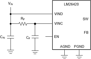
LM26420-Q1 30069638.gifFigure 29. RC Filter On VINC

In general, RF is typically between 1 Ω and 10 Ω so that the steady state voltage drop across the resistor due to the VINC bias current does not affect the UVLO level. CF can range from 0.22 µF to 1 µF in X7R or X5R dielectric, where the RC time constant should be at least 2 µs. CF must be placed as close to the device as possible with a direct connection from VINC and AGND.