SNVS002E January 1999 – October 2014 LM2662 , LM2663
PRODUCTION DATA.
- 1 Features
- 2 Applications
- 3 Description
- 4 Revision History
- 5 Pin Configuration and Functions
- 6 Specifications
- 7 Parameter Measurement Information
- 8 Detailed Description
- 9 Application and Implementation
- 10Power Supply Recommendations
- 11Layout
- 12Device and Documentation Support
- 13Mechanical, Packaging, and Orderable Information
Package Options
Mechanical Data (Package|Pins)
- D|8
Thermal pad, mechanical data (Package|Pins)
Orderable Information
1 Features
- Inverts or Doubles Input Supply Voltage
- 3.5-Ω Typical Output Resistance
- 86% Typical Conversion Efficiency at 200 mA
- (LM2662) Selectable Oscillator Frequency: 20 kHz/150 kHz
- (LM2663) Low Current Shutdown Mode
2 Applications
- Laptop Computers
- Cellular Phones
- Medical Instruments
- Operational Amplifier Power Supplies
- Interface Power Supplies
- Handheld Instruments
Voltage Inverter
3 Description
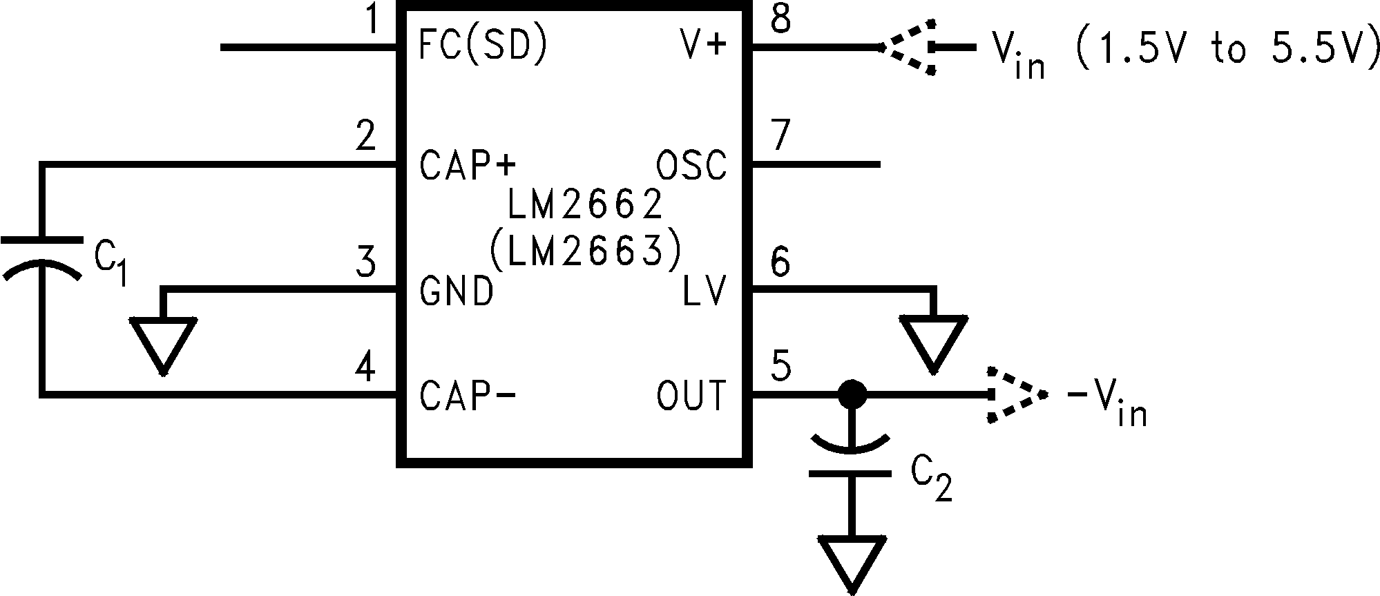
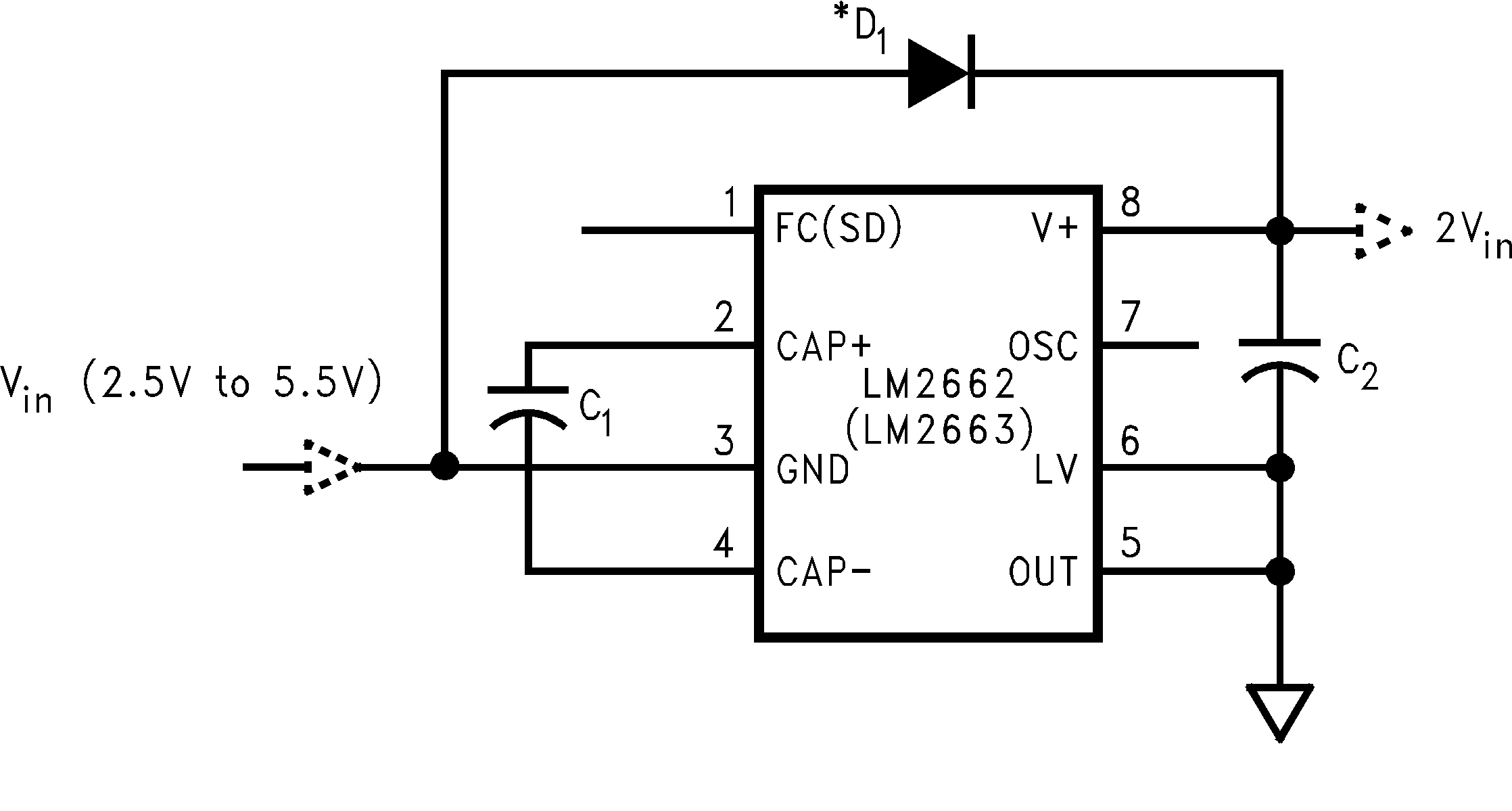
The LM2662/LM2663 CMOS charge-pump voltage converter inverts a positive voltage in the range of 1.5 V to 5.5 V to the corresponding negative voltage. The LM2662/LM2663 uses two low cost capacitors to provide 200 mA of output current without the cost, size, and EMI related to inductor based converters. With an operating current of only 300 μA and operating efficiency greater than 90% at most loads, the LM2662/LM2663 provides ideal performance for battery powered systems. The LM2662/LM2663 may also be used as a positive voltage doubler.
The oscillator frequency can be lowered by adding an external capacitor to the OSC pin. Also, the OSC pin may be used to drive the LM2662/LM2663 with an external clock. For LM2662, a frequency control (FC) pin selects the oscillator frequency of 20 kHz or 150 kHz. For LM2663, an external shutdown (SD) pin replaces the FC pin. The SD pin can be used to disable the device and reduce the quiescent current to 10 μA. The oscillator frequency for LM2663 is 150 kHz.
Device Information(1)
| PART NUMBER | PACKAGE | BODY SIZE (NOM) |
|---|---|---|
| LM2662 | SOIC (8) | 4.90 mm x 3.91 mm |
| LM2663 |
- For all available packages, see the orderable addendum at the end of the datasheet.
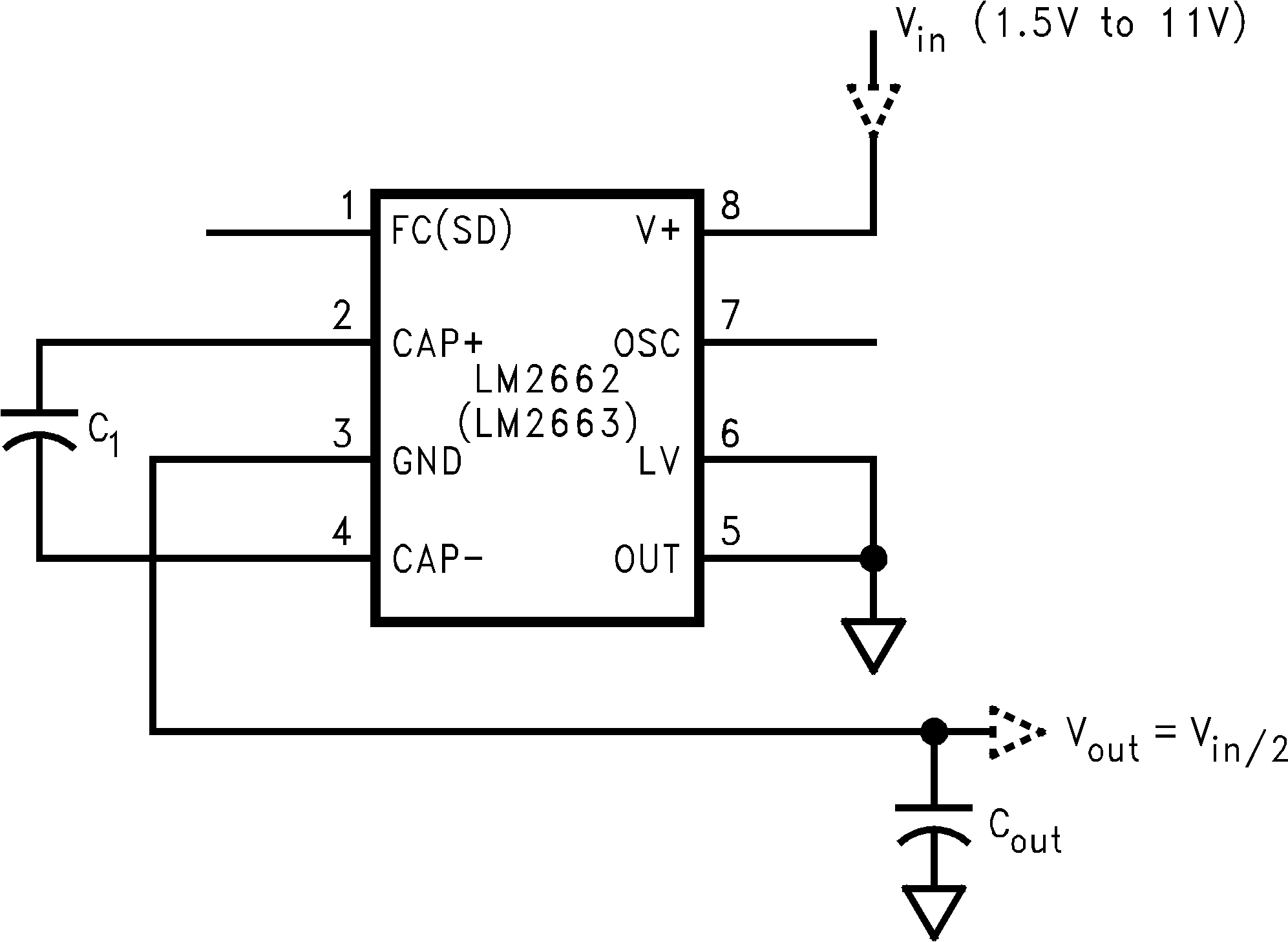
Splitting VIN in Half