SBOS987B August   2020  – October 2021 LM2902LV-Q1 , LM2904LV-Q1

PRODUCTION DATA  

  1. Features
  2. Applications
  3. Description
  4. Revision History
  5. Pin Configuration and Functions
  6. Specifications
    1. 6.1 Absolute Maximum Ratings
    2. 6.2 ESD Ratings
    3. 6.3 Recommended Operating Conditions
    4. 6.4 Thermal Information: LM2904LV-Q1
    5. 6.5 Thermal Information: LM2902LV-Q1
    6. 6.6 Electrical Characteristics
    7. 6.7 Typical Characteristics
  7. Detailed Description
    1. 7.1 Overview
    2. 7.2 Functional Block Diagram
    3. 7.3 Feature Description
      1. 7.3.1 Operating Voltage
      2. 7.3.2 Common-Mode Input Range Includes Ground
      3. 7.3.3 Overload Recovery
      4. 7.3.4 Electrical Overstress
      5. 7.3.5 EMI Susceptibility and Input Filtering
    4. 7.4 Device Functional Modes
  8. Application and Implementation
    1. 8.1 Application Information
    2. 8.2 Typical Application
      1. 8.2.1 Design Requirements
      2. 8.2.2 Detailed Design Procedure
      3. 8.2.3 Application Curve
  9. Power Supply Recommendations
    1. 9.1 Input and ESD Protection
  10. 10Layout
    1. 10.1 Layout Guidelines
    2. 10.2 Layout Example
  11. 11Device and Documentation Support
    1. 11.1 Documentation Support
      1. 11.1.1 Related Documentation
    2. 11.2 Related Links
    3. 11.3 Receiving Notification of Documentation Updates
    4. 11.4 Support Resources
    5. 11.5 Trademarks
    6. 11.6 Electrostatic Discharge Caution
    7. 11.7 Glossary
  12. 12Mechanical, Packaging, and Orderable Information

Package Options

Mechanical Data (Package|Pins)
Thermal pad, mechanical data (Package|Pins)
Orderable Information

Detailed Design Procedure

The transfer function of the circuit in Figure 8-1 is given in Equation 1:

Equation 1. GUID-55791B5C-190A-4DF4-B254-3CC786FBF411-low.gif

The load current (ILOAD) produces a voltage drop across the shunt resistor (RSHUNT). The load current is set from 0 A to 1 A. To keep the shunt voltage below 100 mV at maximum load current, the largest allowable shunt resistor is shown using Equation 2:

Equation 2. GUID-C45013C6-1441-4BF9-AF6C-656A61F6F3B0-low.gif

Using Equation 2, RSHUNT is calculated to be 100 mΩ. The voltage drop produced by ILOAD and RSHUNT is amplified by the LM290xLV-Q1 device to produce an output voltage of approximately 0 V to 3.5 V. The gain needed by the LM290xLV-Q1 to produce the necessary output voltage is calculated using Equation 3:

Equation 3. GUID-DEB413BB-9F8B-46D5-947C-A6001295FF71-low.gif

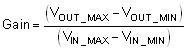
Using Equation 3, the required gain is calculated to be 35 V/V, which is set with resistors RF and RG. Equation 4 sizes the resistors RF and RG, to set the gain of the LM290xLV-Q1 device to 35 V/V.

Equation 4. GUID-D7251FDF-DA40-4323-8F1C-8EDCDE56A220-low.gif