SNOSBJ6G October 1999 – October 2018 LM193-N , LM2903-N , LM293-N , LM393-N
PRODUCTION DATA.
- 1 Features
- 2 Applications
- 3 Description
- 4 Revision History
- 5 Pin Configuration and Functions
-
6 Specifications
- 6.1 Absolute Maximum Ratings
- 6.2 ESD Ratings
- 6.3 Recommended Operating Conditions
- 6.4 Thermal Information
- 6.5 Electrical Characteristics: LM193A V+= 5 V, TA = 25°C
- 6.6 Electrical Characteristics: LM193A (V+ = 5 V)
- 6.7 Electrical Characteristics: LMx93 and LM2903 V+= 5 V, TA = 25°C
- 6.8 Electrical Characteristics: LMx93 and LM2903 (V+ = 5 V)
- 6.9 Typical Characteristics: LMx93 and LM193A
- 6.10 Typical Characteristics: LM2903
- 7 Detailed Description
- 8 Application and Implementation
- 9 Power Supply Recommendations
- 10Layout
- 11Device and Documentation Support
- 12Mechanical, Packaging, and Orderable Information
Package Options
Mechanical Data (Package|Pins)
Thermal pad, mechanical data (Package|Pins)
Orderable Information
5 Pin Configuration and Functions
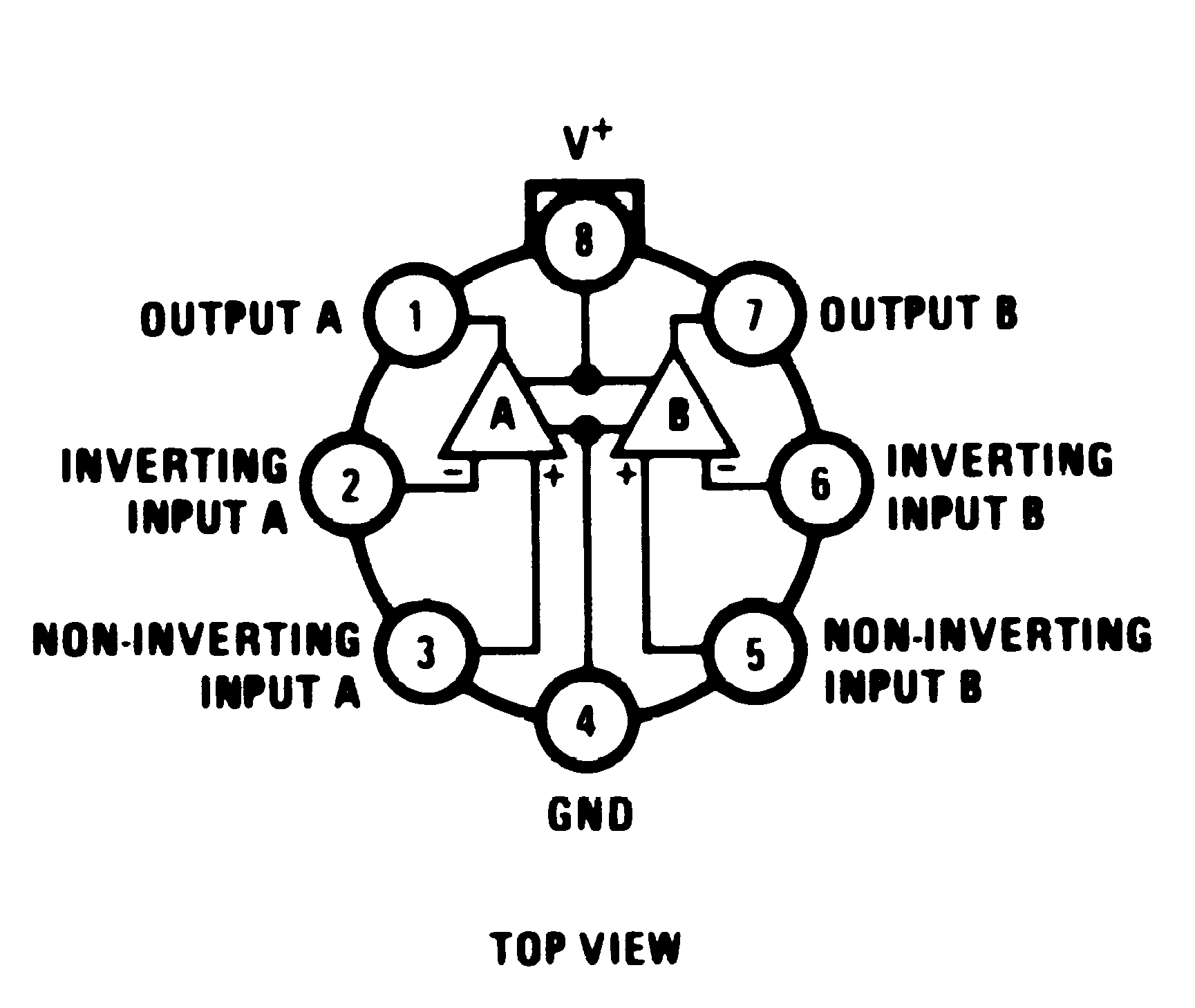
LMC Package
8-Pin TO-99
Top View

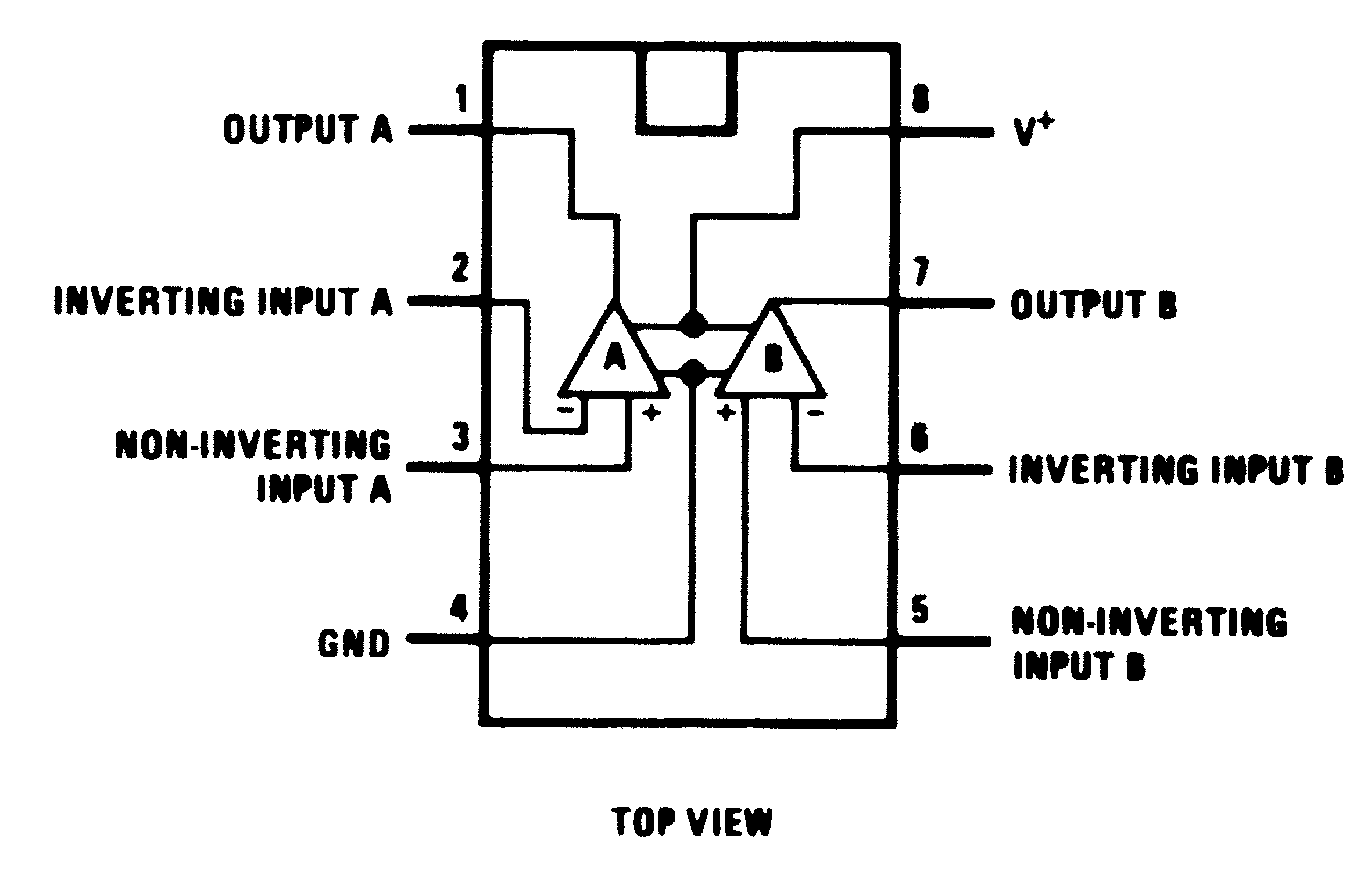
P and D Package
8-Pin CDIP, PDIP, SOIC
Top View

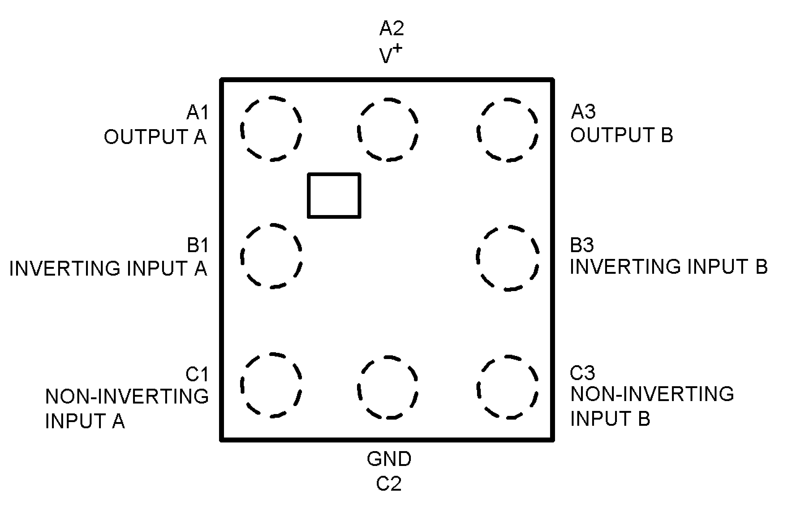
YZR Package
8-Pin DSBGA
Top View

Pin Functions
| PIN | I/O | DESCRIPTION | ||
|---|---|---|---|---|
| NAME | NO. | |||
| PDIP/SOIC/TO-99 | DSBGA | |||
| OUTA | 1 | A1 | O | Output, Channel A |
| -INA | 2 | B1 | I | Inverting Input, Channel A |
| +INA | 3 | C1 | I | Noninverting Input, Channel A |
| GND | 4 | C2 | P | Ground |
| +INB | 5 | C3 | I | Noninverting Input, Channel B |
| -INB | 6 | B3 | I | Inverting Input, Channel B |
| OUTB | 7 | A3 | O | Output, Channel B |
| V+ | 8 | A2 | P | Positive power supply |