SNOSBJ6G October 1999 – October 2018 LM193-N , LM2903-N , LM293-N , LM393-N
PRODUCTION DATA.
- 1 Features
- 2 Applications
- 3 Description
- 4 Revision History
- 5 Pin Configuration and Functions
-
6 Specifications
- 6.1 Absolute Maximum Ratings
- 6.2 ESD Ratings
- 6.3 Recommended Operating Conditions
- 6.4 Thermal Information
- 6.5 Electrical Characteristics: LM193A V+= 5 V, TA = 25°C
- 6.6 Electrical Characteristics: LM193A (V+ = 5 V)
- 6.7 Electrical Characteristics: LMx93 and LM2903 V+= 5 V, TA = 25°C
- 6.8 Electrical Characteristics: LMx93 and LM2903 (V+ = 5 V)
- 6.9 Typical Characteristics: LMx93 and LM193A
- 6.10 Typical Characteristics: LM2903
- 7 Detailed Description
- 8 Application and Implementation
- 9 Power Supply Recommendations
- 10Layout
- 11Device and Documentation Support
- 12Mechanical, Packaging, and Orderable Information
Package Options
Mechanical Data (Package|Pins)
Thermal pad, mechanical data (Package|Pins)
Orderable Information
8.2.2.2 V+ = 5.0 VDC Application Circuits
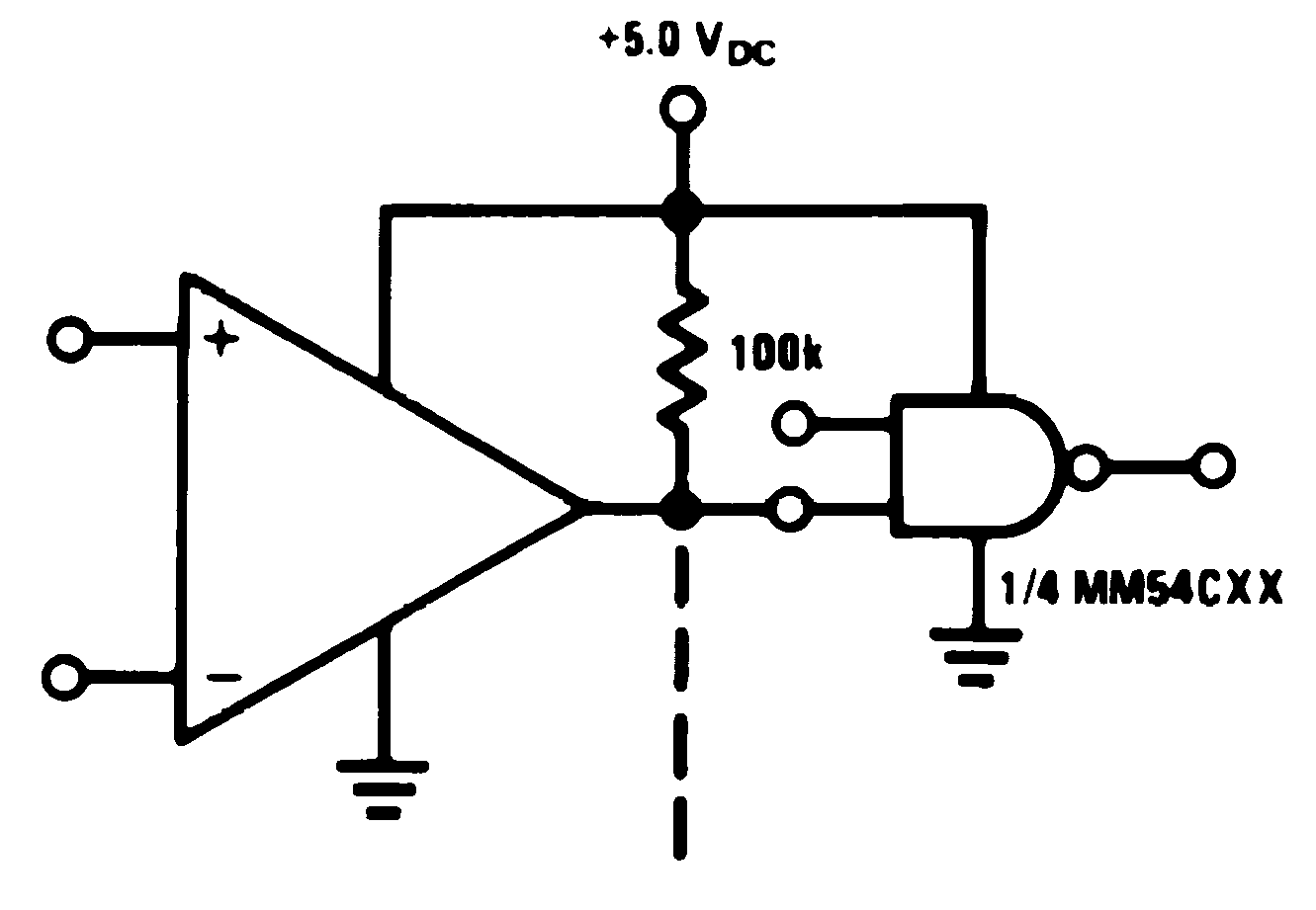 Figure 15. Driving CMOS
 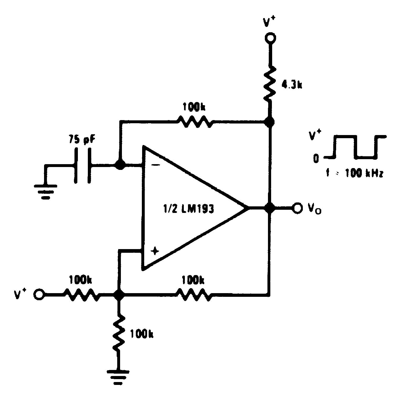 Figure 17. Squarewave Oscillator
 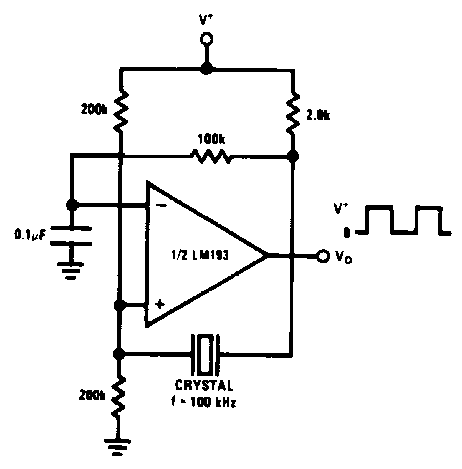 Figure 19. Crystal Controlled Oscillator
 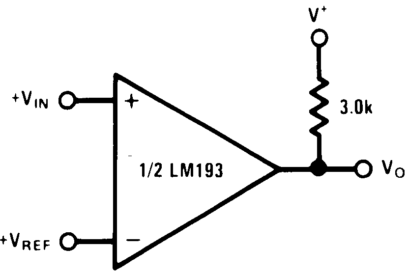 Figure 21. Basic Comparator
 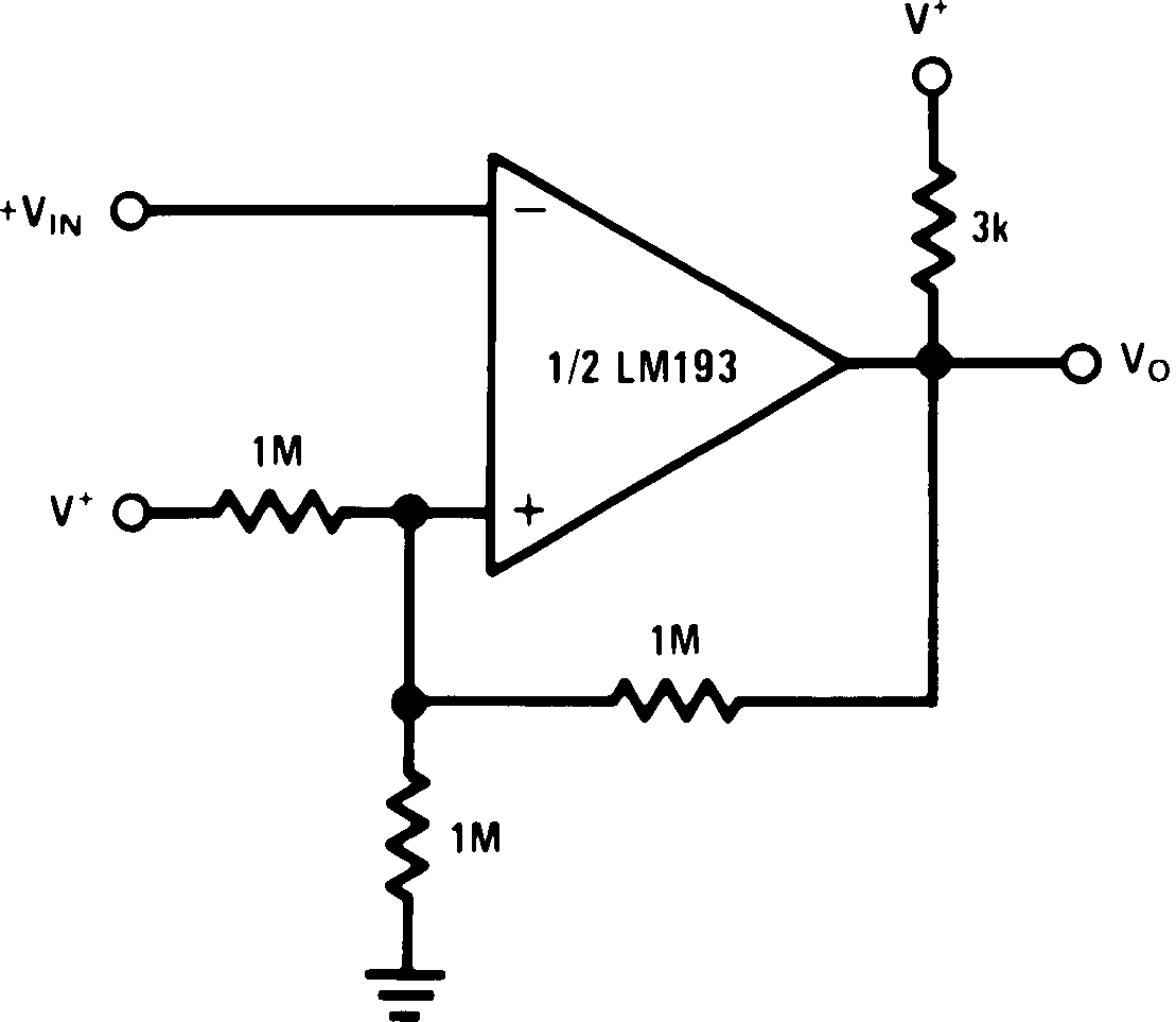 Figure 23. Inverting Comparator With Hysteresis
 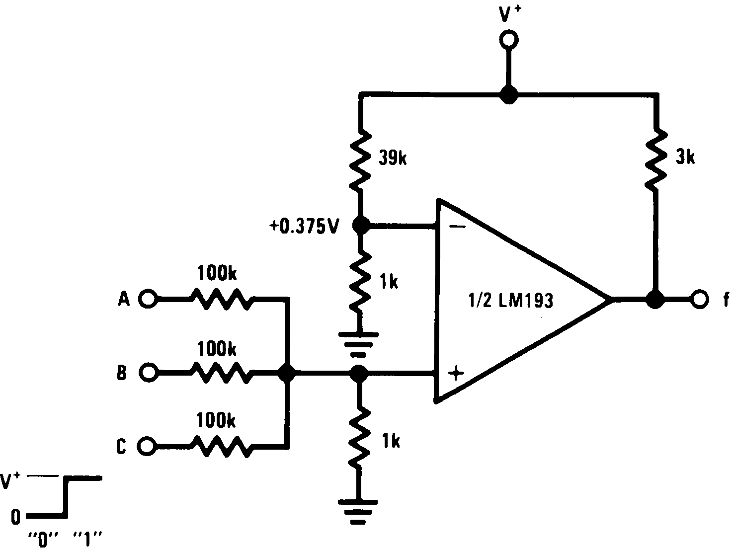 Figure 25. And Gate
 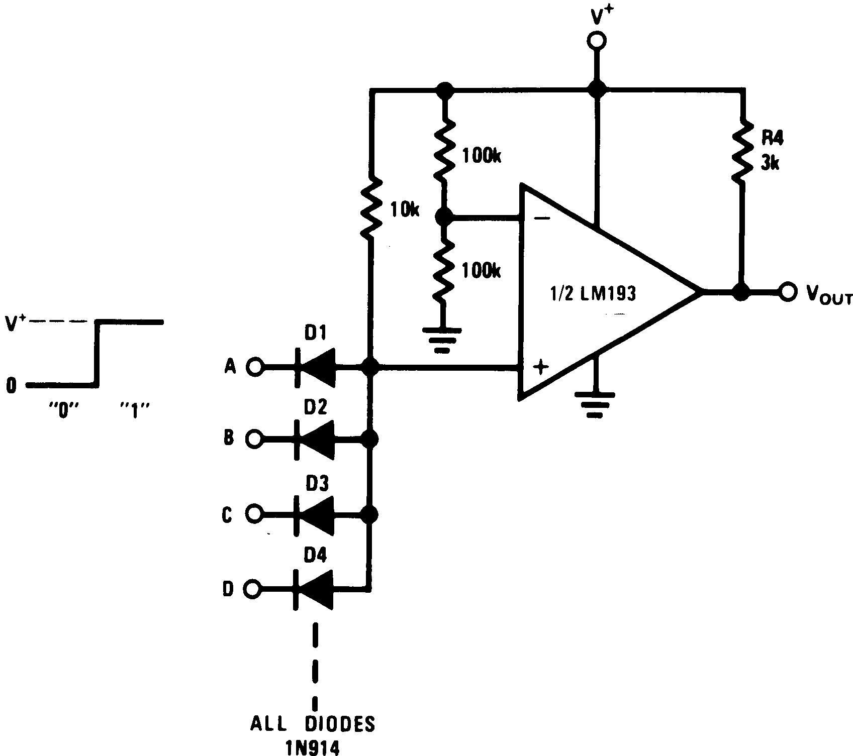 Figure 27. Large Fan-In and Gate
 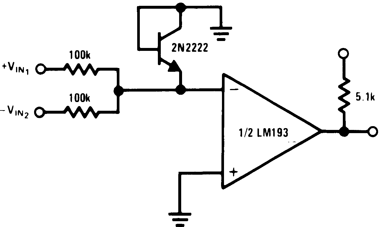 Figure 29. Comparing Input Voltages of Opposite Polarity
 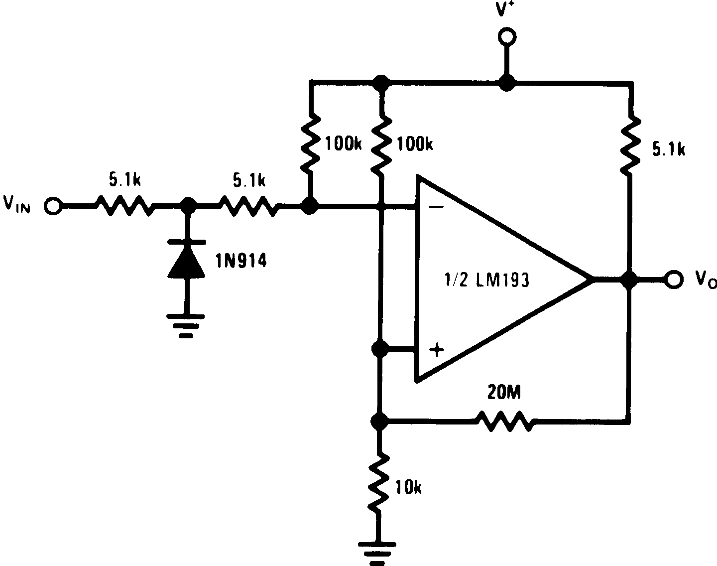 Figure 31. Zero Crossing Detector (Single Power Supply)
 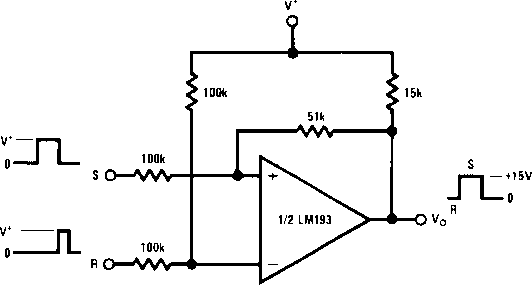 Figure 33. Bi-Stable Multivibrator
 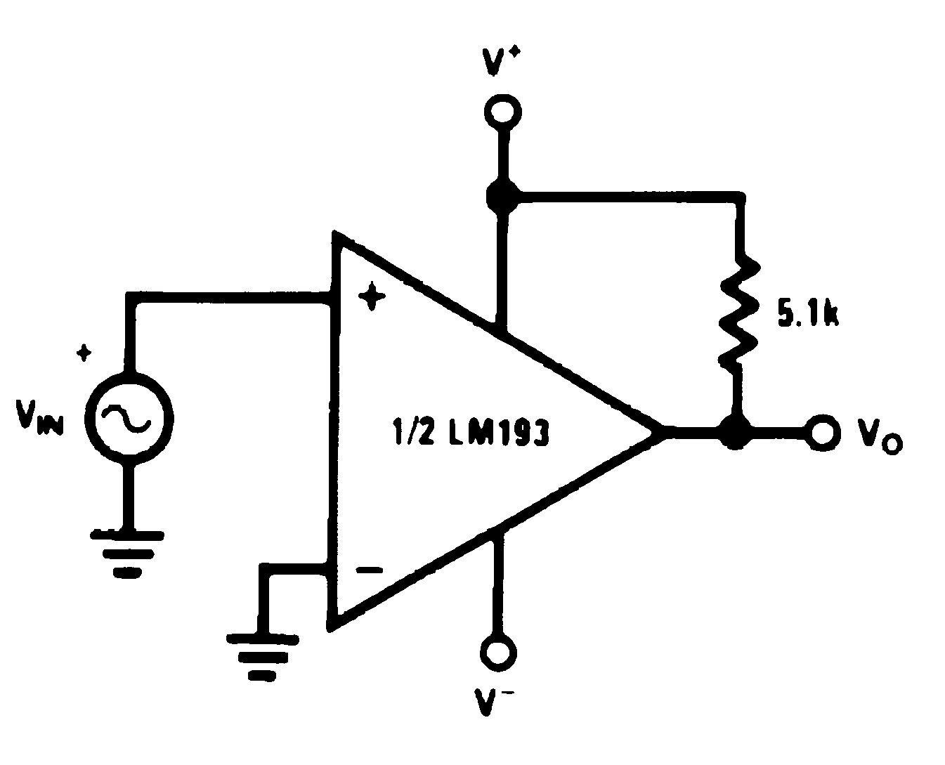 Figure 35. Zero Crossing Detector
 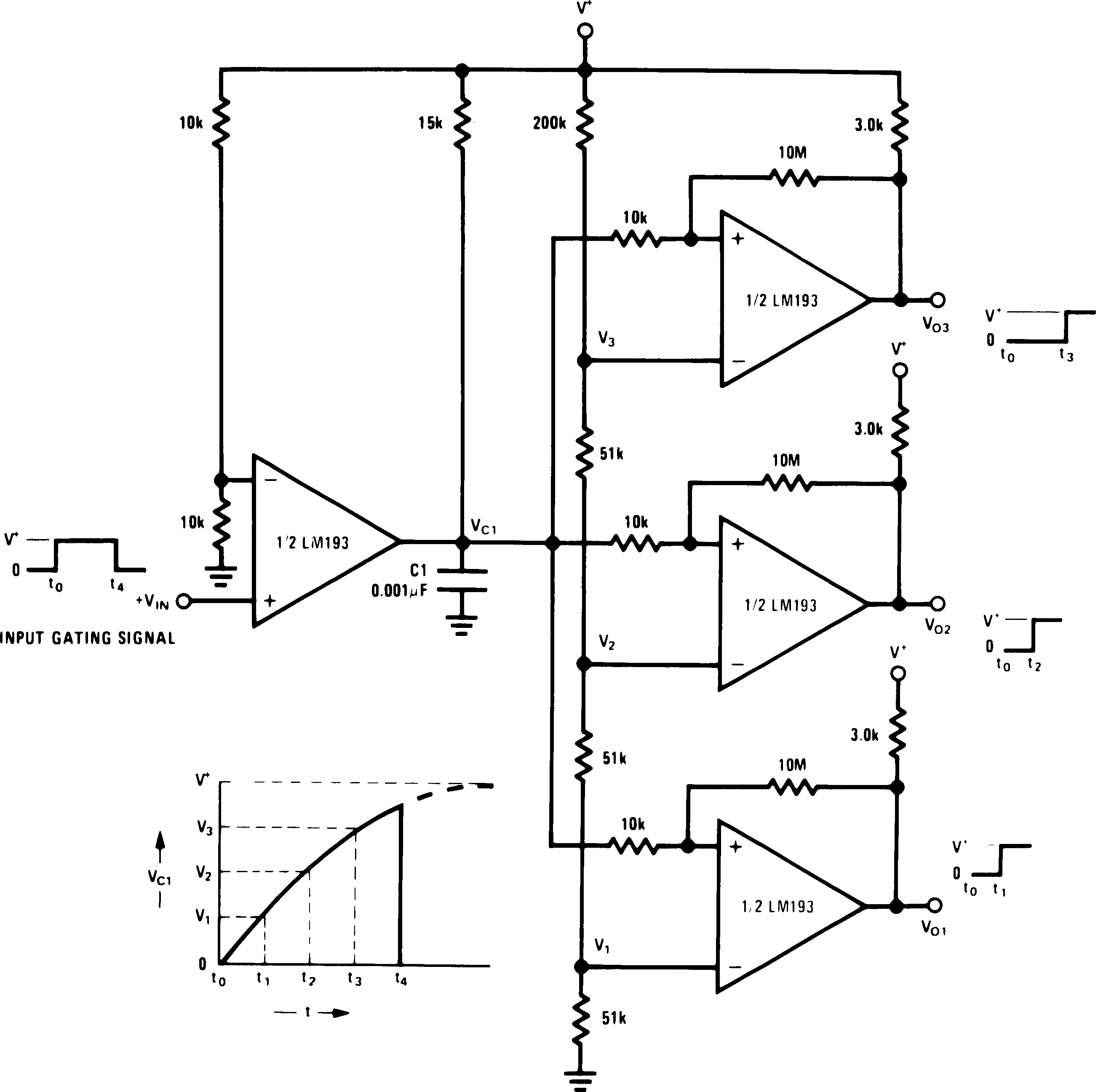 Figure 37. Time Delay Generator
 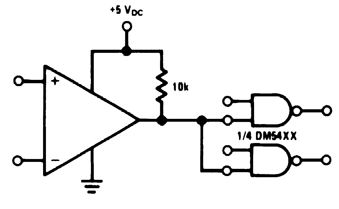 Figure 16. Driving TTL
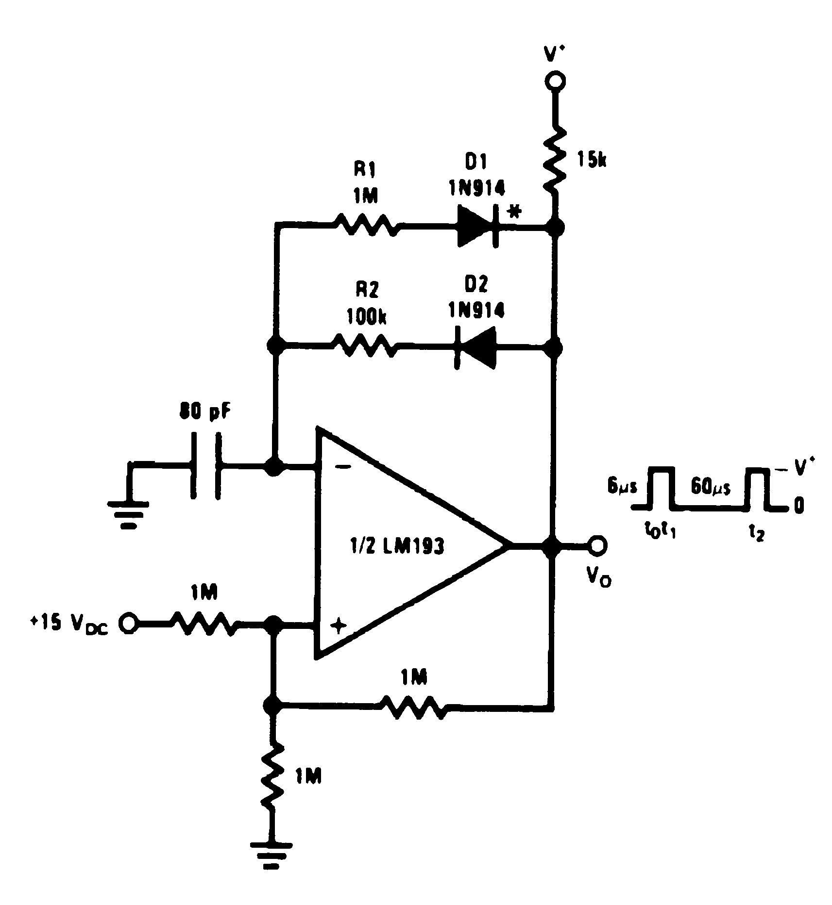
| * For large ratios of R1/R2, | ||
| D1 can be omitted. |
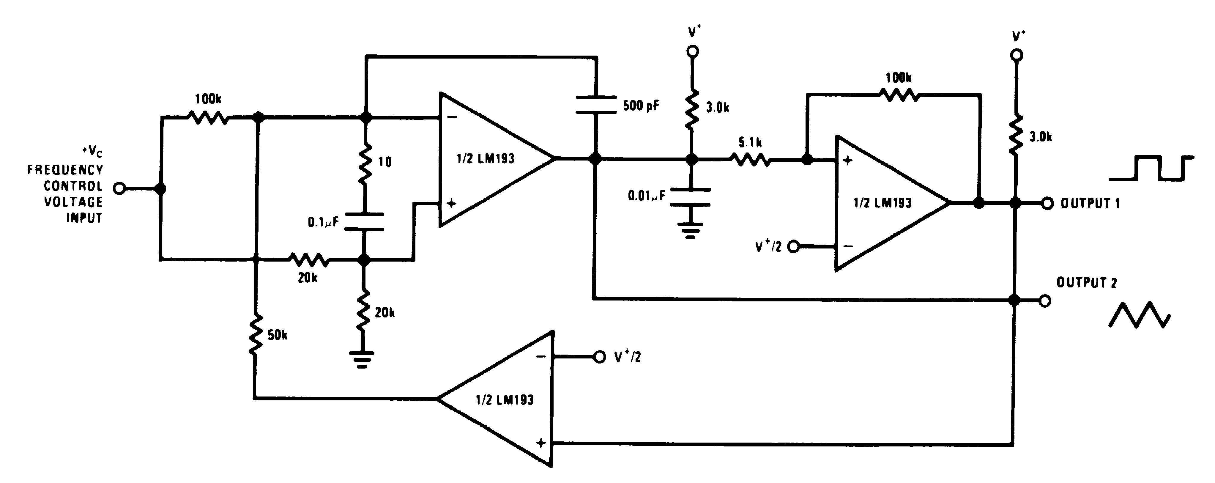
| V* = +30 VDC | ||
| +250 mVDC ≤ VC ≤ +50 VDC | ||
| 700Hz ≤ fo ≤ 100kHz |
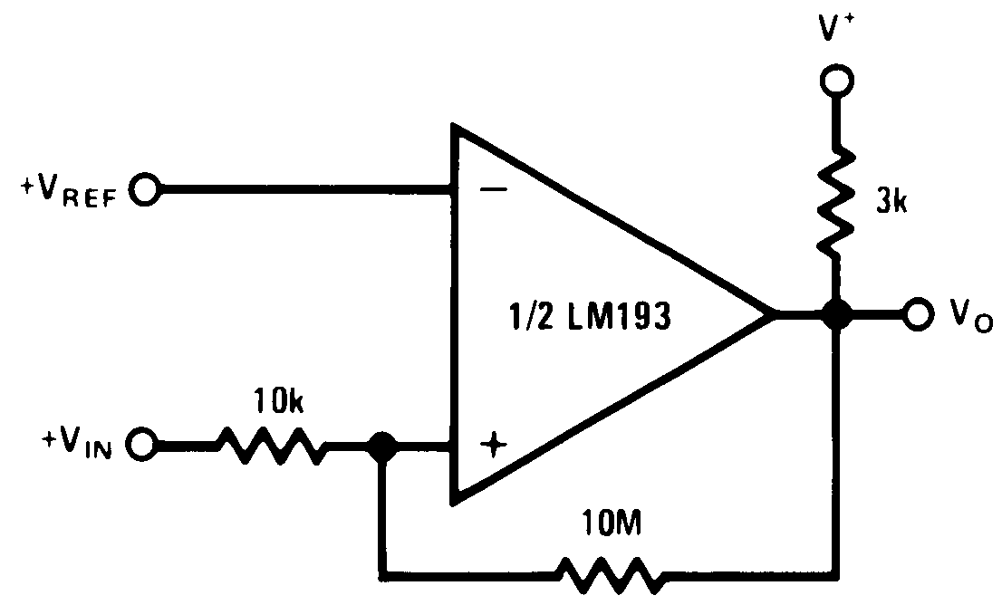 Figure 22. Non-Inverting Comparator With Hysteresis
 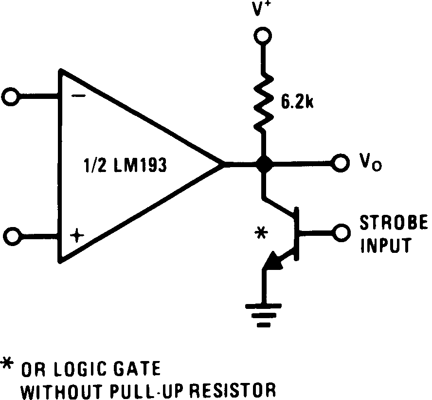 Figure 24. Output Strobing
 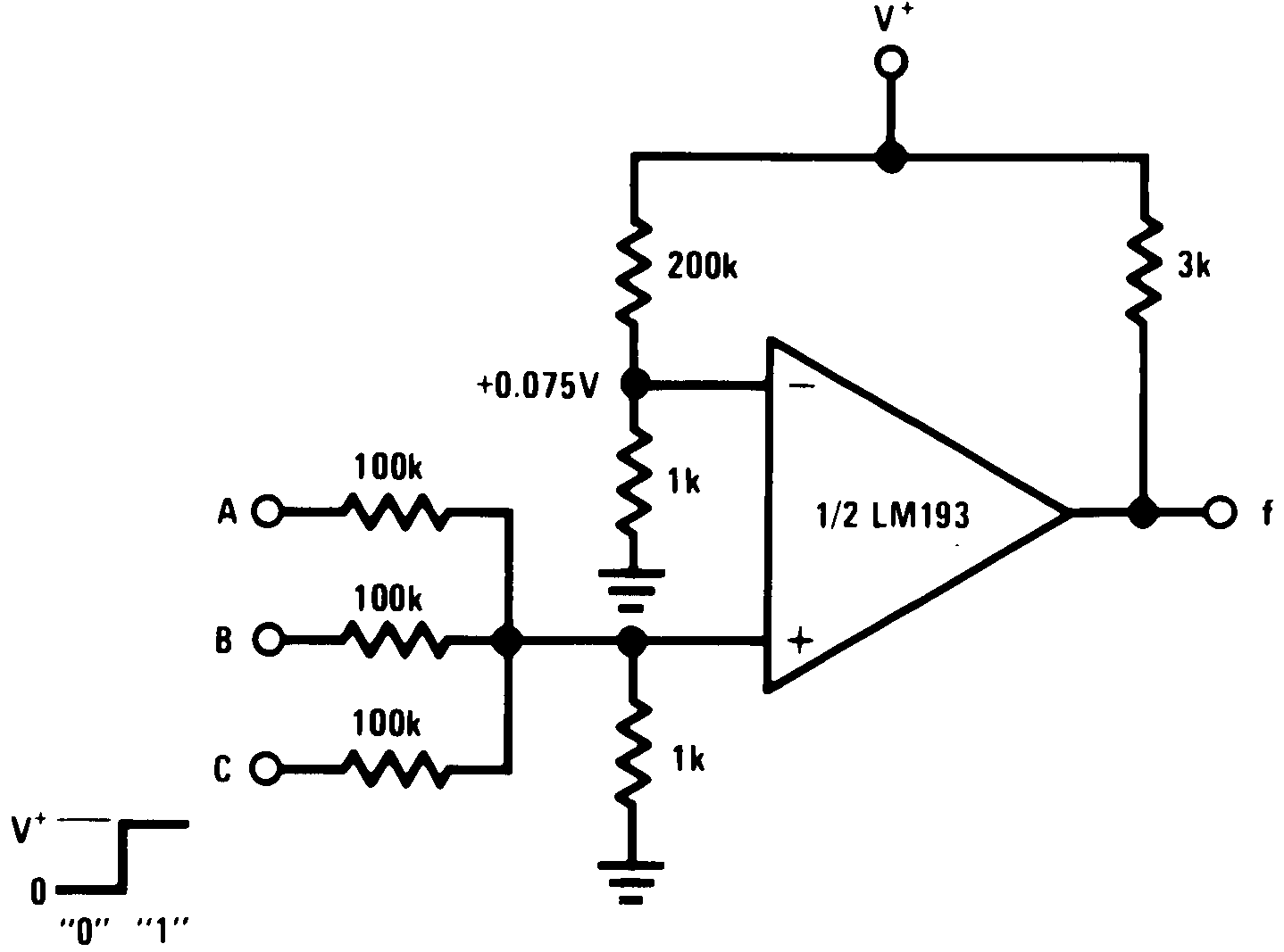 Figure 26. Or Gate
 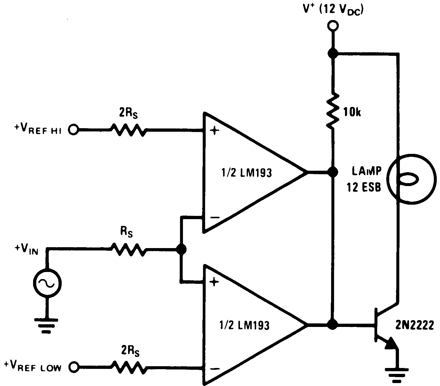 Figure 28. Limit Comparator
 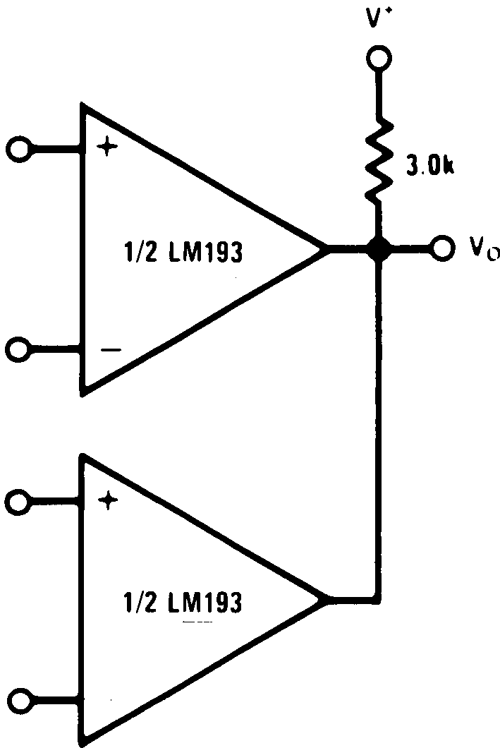 Figure 30. Oring the Outputs
 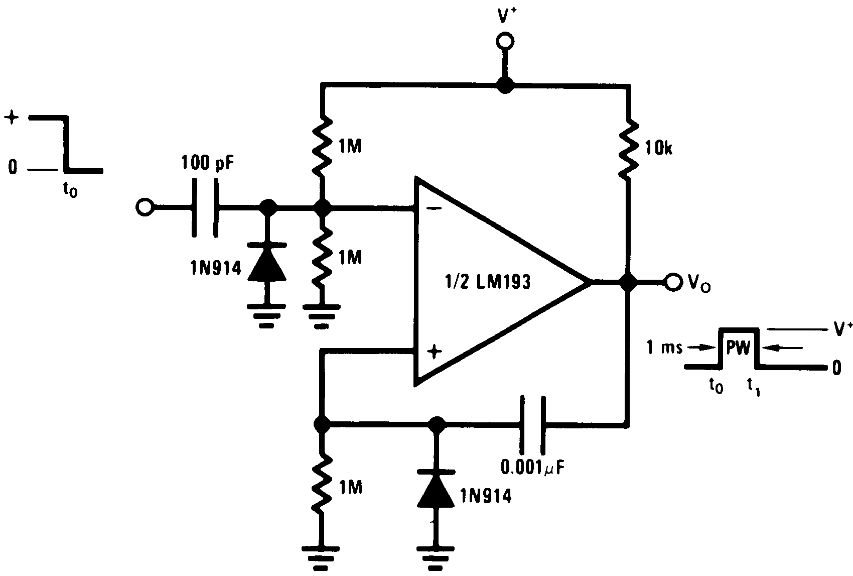 Figure 32. One-Shot Multivibrator
 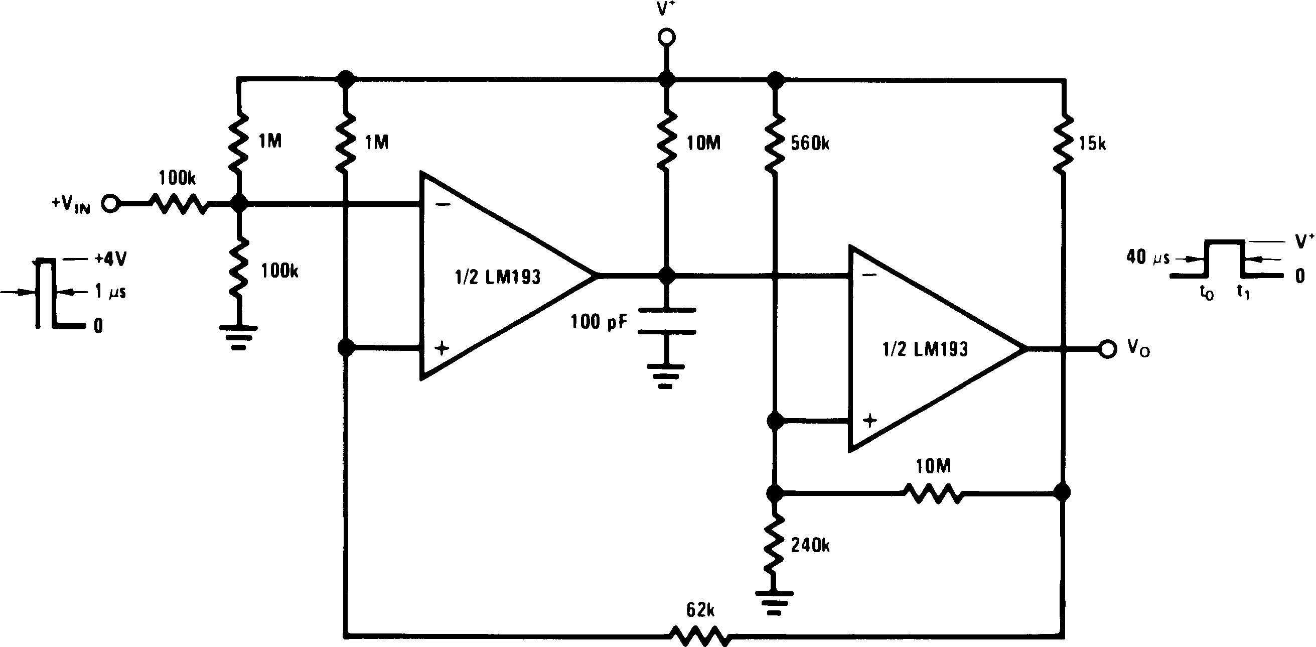 Figure 34. One-Shot Multivibrator With Input Lock Out
 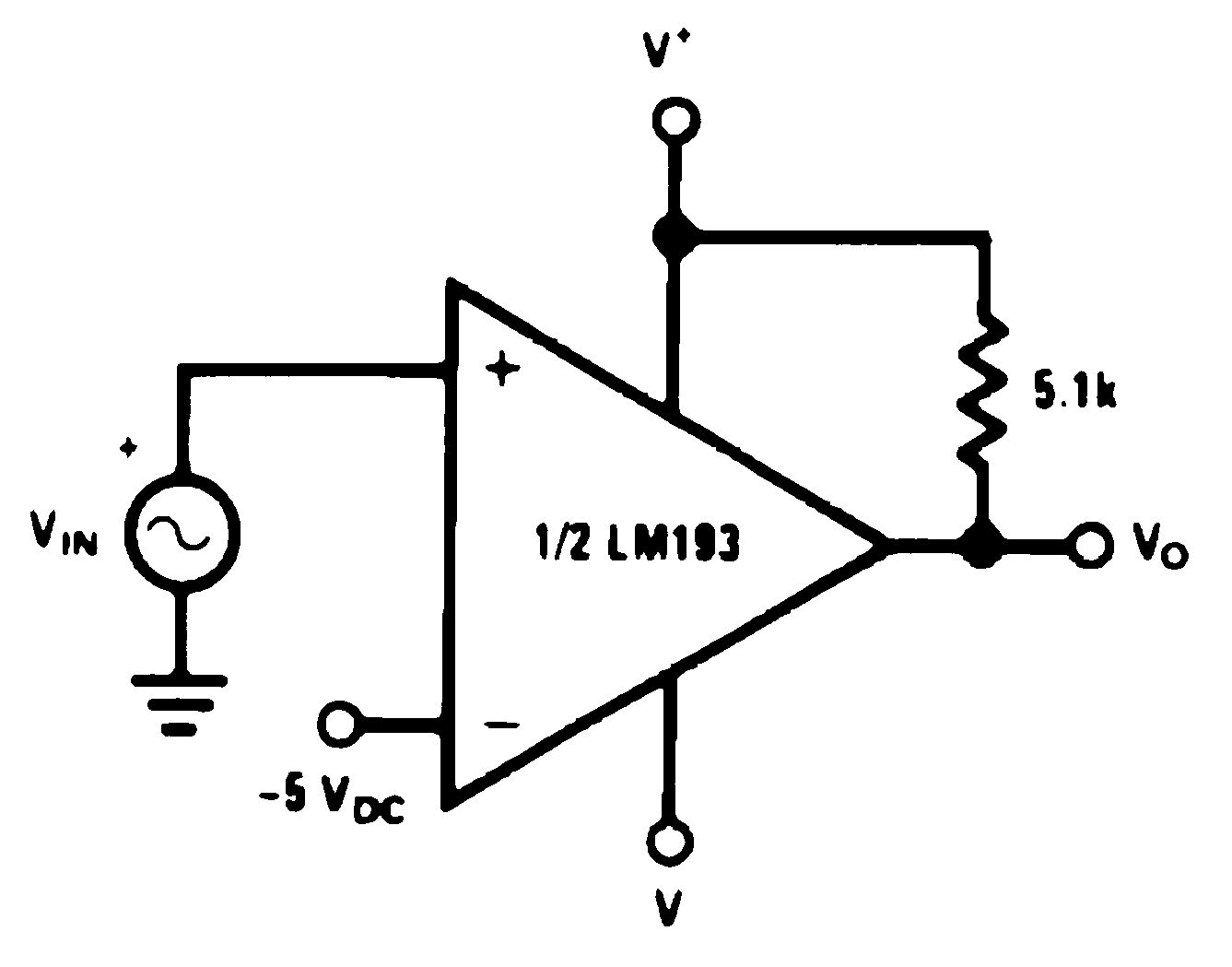 Figure 36. Comparator With a Negative Reference