SNVS775L March 2000 – January 2018 LM317L-N
PRODUCTION DATA.
- 1 Features
- 2 Applications
- 3 Description
- 4 Revision History
- 5 Pin Configuration and Functions
- 6 Specifications
- 7 Detailed Description
-
8 Application and Implementation
- 8.1 Application Information
- 8.2
Typical Applications
- 8.2.1 1.25-V to 25-V Adjustable Regulator
- 8.2.2 Digitally-Selected Outputs
- 8.2.3 High Gain Amplifier
- 8.2.4 Adjustable Current Limiter
- 8.2.5 Precision Current Limiter
- 8.2.6 Slow Turnon 15-V Regulator
- 8.2.7 Adjustable Regulator With Improved Ripple Rejection
- 8.2.8 High Stability 10-V Regulator
- 8.2.9 Adjustable Regulator With Current Limiter
- 8.2.10 0-V to 30-V Regulator
- 8.2.11 Regulator With 15-mA Short-Circuit Current
- 8.2.12 Power Follower
- 8.2.13 Adjusting Multiple On-Card Regulators With Single Control
- 8.2.14 100-mA Current Regulator
- 8.2.15 1.2-V to 12-V Regulator With Minimum Program Current
- 8.2.16 50-mA Constant Current Battery Charger for Nickel-Cadmium Batteries
- 8.2.17 5-V Logic Regulator With Electronic Shutdown
- 8.2.18 Current-Limited 6-V Charger
- 8.2.19 Short Circuit-Protected 80-V Supply
- 8.2.20 Basic High-Voltage Regulator
- 8.2.21 Precision High-Voltage Regulator
- 8.2.22 Tracking Regulator
- 8.2.23 Regulator With Trimmable Output Voltage
- 8.2.24 Precision Reference With Short-Circuit Proof Output
- 8.2.25 Fully-Protected (Bulletproof) Lamp Driver
- 8.2.26 Lamp Flasher
- 9 Power Supply Recommendations
- 10Layout
- 11Device and Documentation Support
- 12Mechanical, Packaging, and Orderable Information
Package Options
Mechanical Data (Package|Pins)
Thermal pad, mechanical data (Package|Pins)
Orderable Information
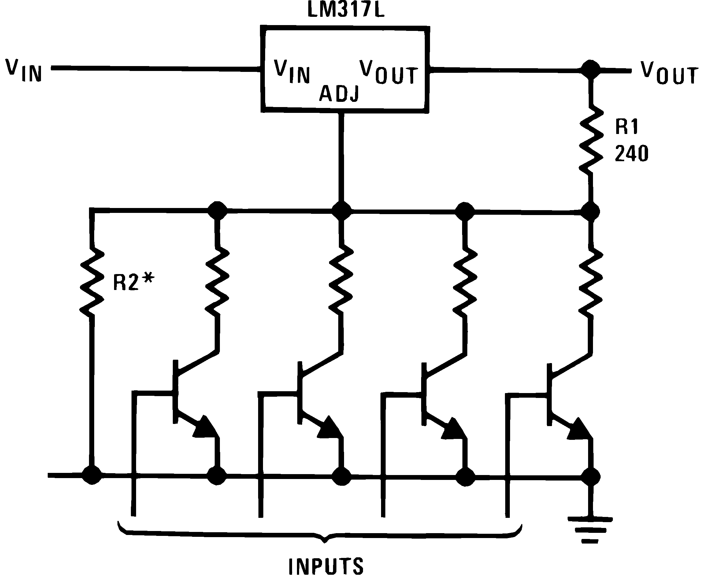
8.2.2 Digitally-Selected Outputs
Figure 18 demonstrates a digitally-selectable output voltage. In its default state, all transistors are off and the output voltage is set based on R1 and R2. By driving certain transistors, the associated resistor is connected in parallel to R2, modifying the output voltage of the regulator.

*Sets maximum VOUT
Figure 18. Digitally-Selected Outputs