SNVS678F June 2010 – November 2015 LM3414 , LM3414HV
PRODUCTION DATA.
- 1 Features
- 2 Applications
- 3 Description
- 4 Revision History
- 5 Pin Configuration and Functions
- 6 Specifications
- 7 Detailed Description
- 8 Application and Implementation
- 9 Power Supply Recommendations
- 10Layout
- 11Device and Documentation Support
- 12Mechanical, Packaging, and Orderable Information
Package Options
Mechanical Data (Package|Pins)
Thermal pad, mechanical data (Package|Pins)
- DDA|8
Orderable Information
7 Detailed Description
7.1 Overview
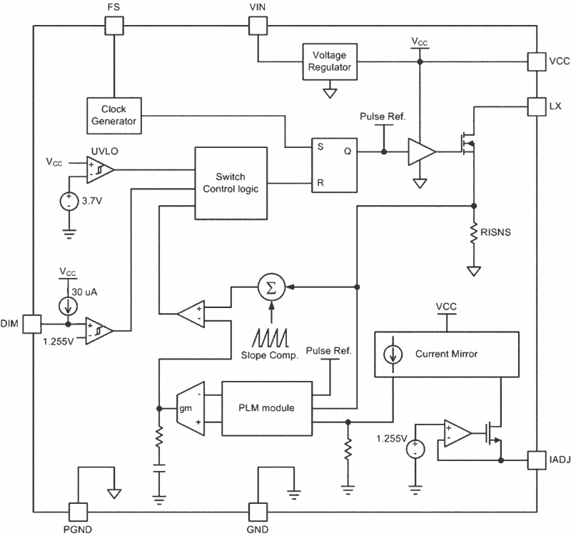
The LM3414/HV is a high power floating buck LED driver with wide input voltage ranges. The device requires no external current sensing elements and loop compensation networks. The integrated power N-MOSFET enables high-output power with up to 1000-mA output current. The combination of Pulse Width Modulation (PWM), control architecture, and the proprietary Pulse Level Modulation (PLM) ensures accurate current regulation, good EMI performance, and provides high flexibility on inductor selection. High-speed dimming control input allows precision and high resolution brightness control for applications require fine brightness adjustment.
7.2 Functional Block Diagram
7.3 Feature Description
7.3.1 Pulse-Level-Modulation (PLM) Operation Principles
The main control circuitry of the LM3414/HV is generally a Pulse-Width-Modulated (PWM) controller with the incorporation of the Pulse-Level-Modulation (PLM) technology. PLM is a technology that facilitates true output average current control without the need to sense the output current directly. In the LM3414/LM3414HV, the PLM circuit senses the current of the internal switch through integrated current sensing circuitry to realize average output current control. The use of PLM reduces the current sensing power losses as it needs current information only when the switch is turned ON. For proper operation of this control scheme, the converter must operate in CCM (continuous conduction mode), so the switching frequency and inductor value must be chosen to prevent the inductor current reaching 0 A during the switch OFF time each cycle.
In general, for the LED drivers with current sensing resistor at the output, the power dissipation on the current sensing resistor is ILED2 × RISNS, where ILED is the average output current and RISNS is the resistance of the current sensing resistor. In the LM3414/LM3414HV, power dissipates on the internal RISNS only during ON period of the internal power switch. The power loss on RISNS(internal) becomes ILED2 × RISNS × D, where D is the switching duty cycle. For example, when the switching duty cycle, D of a converter is 0.5, the power loss on RISNS with PLM is half of those with conventional output current sensing resulting in increased efficiency.
The Pulse-Level-Modulation is a patented method to ensure accurate average output current regulation without the need of direct output current sensing. Figure 14 shows the current waveforms of a typical buck converter under steady state, where, IL1 is the inductor current and ILX is the main switch current flowing into the LX pin. For a buck converter operating in steady state, the mid-point of the RAMP section of the main switch current is equal to the average level of the inductor current–hence the average output current. In short, by regulating the mid-point of the RAMP section of the main switch current with respect to a precise reference level, PLM achieves output current regulation by sensing the main switch current solely.
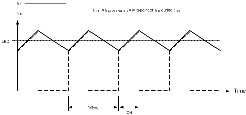 Figure 14. Waveforms of a Floating Buck LED Driver With PLM
7.3.2 Minimum Switch ON-time
As the LM3414 features a 400 ns minimum ON time, it is essential to make sure the ON time of the internal switch is not shorter than 400 ns when setting the LED driving current. If the switching ON time is shorter than 400 ns, the accuracy of the LED current may not maintain and exceed the rated current of the LEDs. The ratio of the LED forward voltage to input voltage is restricted by the following restriction, as shown in Equation 1.

7.3.3 Peak Switch Current Limit
The LM3414/HV features an integrated switch current limiting mechanism that protects the LEDs from being overdriven. The switch current limiter triggers when the switch current exceeds three times the current level set by RIADJ. Once the current limiter is triggered, the internal power switch turns OFF for 3.6 µs to allow the inductor to discharge and cycles repetitively until the overcurrent condition is removed. The current limiting feature is exceptionally important to avoid permanent damage of the LM3414/HV application circuit due to short circuit of LED string.
7.3.4 PWM Dimming Control
The DIM pin of the LM3414/HV is an input with internal pullup that accepts logic signals for average LED current control. Applying a logic high (greater than 1.2 V) signal to the DIM pin or leaving the DIM pin open will enable the device. Applying a logic low signal (less than 0.9 V) to the DIM pin will disable the switching activity of the device but maintain VCC regulator active. The LM3414/HV allows the inductor current to slew up to the preset regulated level at full speed instead of charging the inductor with multiple restrained switching duty cycles. This enables the LM3414/HV to achieve high-speed dimming and very fine dimming control as shown in Figure 15 and Figure 16.
 Figure 15. LED Current Slew Up With Multiple Switching Cycle
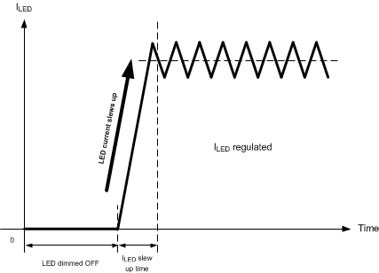 Figure 16. Shortened Current Slew Up Time of the LM3414/HV
To ensure normal operation of the LM3414/HV, TI recommends setting the dimming frequency not higher than 1/10 of the switching frequency. The minimum dimming duty cycle is limited by the 400 ns minimum ON time. In applications that require high dimming contrast ratio, low dimming frequency should be used.
7.3.5 Analog Dimming Control
The IADJ pin can be used as an analog dimming signal input. As the average output current of the LM3414 depends on the current being drawn from the IADJ pin, thus the LED current can be increased or decreased by applying external bias current to the IADJ pin. The simplified circuit diagram for facilitating analog dimming is as shown in Figure 17. The minimum LED current for analog dimming is 100 mA and the converter must remain in continuous conduction mode (CCM). The switching frequency and inductor value must be sized accordingly.
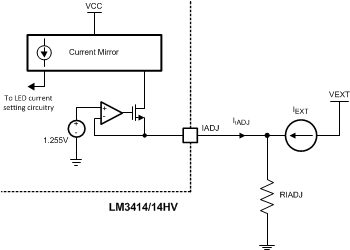 Figure 17. Analog LED Current Control Circuit
When external bias current IEXT is applied to the IADJ pin, the reduction of LED current follows Equation 2 through Equation 3.

Provided that

ILED decreases linearly as IEXT increases.
This feature is exceptionally useful for the applications with analog dimming control signals such as those from analog temperature sensors and ambient light sensors.
Figure 18 shows an example circuit for analog dimming control using simple external biasing circuitry with a variable resistor.
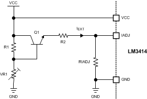 Figure 18. Example Analog Dimming Control Circuit
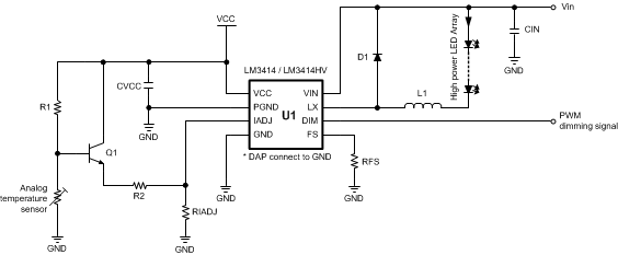
In Figure 18, the variable resistor VR1 controls the base voltage of Q1 and eventually adjusts the bias voltage of current to the IADJ pin (IEXT). As the resistance of VR1 increases and the voltage across VR1 exceeds 1.255 V + 0.7 V, the LED current starts to decrease as IEXT increases.
Where

The analog dimming begins only when IEXT > 0.
7.3.6 Internal VCC Regulator
The LM3414/HV features a 5.4-V internal voltage regulator that connects between the VIN and VCC pins for powering internal circuitry and provide biases to external components. The VCC pin must be bypassed to the GND pin with a 1-µF ceramic capacitor, CVCC that connected to the pins as close as possible. When the input voltage falls to less than 6 V, the VCC voltage will drop to less than 5.4 V and decrease proportionally as Vin decreases. The device will shutdown as the VCC voltage falls to less than 3.9 V. When the internal regulator is used to provide bias to external circuitry, it is essential to ensure the current sinks from VCC pin does not exceed 2 mA to maintain correct voltage regulation.
7.4 Device Functional Modes
There are no additional functional modes for this device.
