SNOSDB3E June 2020 – November 2023 LM339LV-Q1 , LM393LV-Q1 , TL331LV-Q1 , TL391LV-Q1
PRODMIX
- 1
- 1 Features
- 2 Applications
- 3 Description
- 4 Pin Configuration and Functions
-
5 Specifications
- 5.1 Absolute Maximum Ratings
- 5.2 ESD Ratings
- 5.3 Recommended Operating Conditions
- 5.4 Thermal Information for TL3x1LV-Q1
- 5.5 Thermal Information, LM393LV-Q1
- 5.6 Thermal Information, LM339LV-Q1
- 5.7 Electrical Characteristics, TL3x1LV-Q1
- 5.8 Switching Characteristics, TL3x1LV-Q1
- 5.9 Electrical Characteristics, LM393LV-Q1
- 5.10 Switching Characteristics, LM393LV-Q1
- 5.11 Electrical Characteristics, LM339LV-Q1
- 5.12 Switching Characteristics, LM339LV-Q1
- 5.13 Typical Characteristics
- 6 Detailed Description
-
7 Application and Implementation
- 7.1 Application Information
- 7.2 Typical Applications
- 7.3 Power Supply Recommendations
- 7.4 Layout
- 8 Device and Documentation Support
- 9 Revision History
- 10Mechanical, Packaging, and Orderable Information
Package Options
Mechanical Data (Package|Pins)
Thermal pad, mechanical data (Package|Pins)
- DGK|8
Orderable Information
7.1.2.2 Non-Inverting Comparator With Hysteresis
A noninverting comparator with hysteresis requires a two-resistor network and a voltage reference (VREF) at the inverting input, as shown in Figure 7-5,
 Figure 7-5 Non-Inverting Configuration With Hysteresis
The equivalent resistor networks when the output is high and low are shown in Figure 7-6 Note that RPU should be considered in series with R2 when the output is high. RPU should be at least 10x less than R2.
 Figure 7-6 Non-Inverting Configuration Resistor Networks
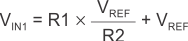
When VIN is less than VREF,, the output is low. For the output to switch from low to high, VIN must rise above the VIN1 threshold. Use Equation 4 to calculate VIN1.
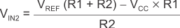
When VIN is greater than VREF, the output is high. For the comparator to switch back to a low state, VIN must drop below VIN2. Use Equation 5 to calculate VIN2.
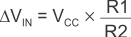
The hysteresis of this circuit is the difference between VIN1 and VIN2, as shown in Equation 6.
For more information, please see Application Notes SNOA997 "Inverting comparator with hysteresis circuit" and SBOA313 "Non-Inverting Comparator With Hysteresis Circuit".