SNOSDA4D June 2020 – November 2023 LM339LV , LM393LV , TL331LV , TL391LV
PRODMIX
- 1
- 1 Features
- 2 Applications
- 3 Description
- 4 Pin Configuration and Functions
-
5 Specifications
- 5.1 Absolute Maximum Ratings
- 5.2 ESD Ratings
- 5.3 Recommended Operating Conditions
- 5.4 Thermal Information for TL3x1LV
- 5.5 Thermal Information, LM393LV
- 5.6 Thermal Information, LM339LV
- 5.7 Electrical Characteristics, TL3x1LV
- 5.8 Switching Characteristics, TL3x1LV
- 5.9 Electrical Characteristics, LM393LV
- 5.10 Switching Characteristics, LM393LV
- 5.11 Electrical Characteristics, LM339LV
- 5.12 Switching Characteristics, LM339LV
- 5.13 Typical Characteristics
- 6 Detailed Description
-
7 Application and Implementation
- 7.1 Application Information
- 7.2 Typical Applications
- 7.3 Power Supply Recommendations
- 7.4 Layout
- 8 Device and Documentation Support
- 9 Revision History
- 10Mechanical, Packaging, and Orderable Information
Package Options
Mechanical Data (Package|Pins)
Thermal pad, mechanical data (Package|Pins)
Orderable Information
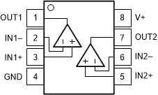
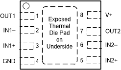
4.2 Pin Functions: LM393LV
 Figure 4-3 D, DGK, PW, DDF Packages
8-Pin SOIC, VSSOP, TSSOP, SOT-23-8
Top View

NOTE: Connect exposed thermal pad directly to GND pin.
Figure 4-4 DSG Package8-Pad WSON With Exposed Thermal Pad
Top View
| PIN | I/O | DESCRIPTION | |
|---|---|---|---|
| NAME | NO. | ||
| OUT1 | 1 | Output | Output pin of the comparator 1 |
| IN1– | 2 | Input | Inverting input pin of comparator 1 |
| IN1+ | 3 | Input | Noninverting input pin of comparator 1 |
GND | 4 | — | Negative supply |
| IN2+ | 5 | Input | Noninverting input pin of comparator 2 |
| IN2– | 6 | Input | Inverting input pin of comparator 2 |
| OUT2 | 7 | Output | Output pin of the comparator 2 |
| V+ | 8 | — | Positive supply |
| Thermal Pad | — | — | Connect directly to GND pin |