SNOSDA4D June 2020 – November 2023 LM339LV , LM393LV , TL331LV , TL391LV
PRODMIX
- 1
- 1 Features
- 2 Applications
- 3 Description
- 4 Pin Configuration and Functions
-
5 Specifications
- 5.1 Absolute Maximum Ratings
- 5.2 ESD Ratings
- 5.3 Recommended Operating Conditions
- 5.4 Thermal Information for TL3x1LV
- 5.5 Thermal Information, LM393LV
- 5.6 Thermal Information, LM339LV
- 5.7 Electrical Characteristics, TL3x1LV
- 5.8 Switching Characteristics, TL3x1LV
- 5.9 Electrical Characteristics, LM393LV
- 5.10 Switching Characteristics, LM393LV
- 5.11 Electrical Characteristics, LM339LV
- 5.12 Switching Characteristics, LM339LV
- 5.13 Typical Characteristics
- 6 Detailed Description
-
7 Application and Implementation
- 7.1 Application Information
- 7.2 Typical Applications
- 7.3 Power Supply Recommendations
- 7.4 Layout
- 8 Device and Documentation Support
- 9 Revision History
- 10Mechanical, Packaging, and Orderable Information
Package Options
Mechanical Data (Package|Pins)
Thermal pad, mechanical data (Package|Pins)
Orderable Information
3 Description
The LV device family consists of single, dual and quad independent voltage comparators that operate from a wide supply voltage range. The LV devices can drop-in replace the standard TL331, LM2xx, LM3xx and LM290x comparator family in low voltage (≤ 5 V) applications for improved performance and added features.
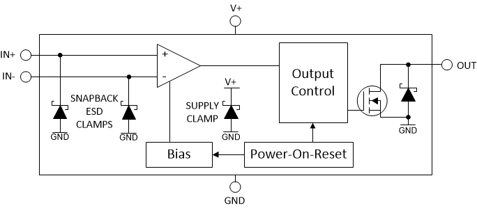
The LV devices include a Power-On-Reset (POR) feature to make sure the output is in a High-Z state until the minimum supply voltage has been reached to prevent output transients during power-up and power-down. The family also feature Rail to Rail inputs that can go up to 6 V without damage or phase inversion.
The LV devices are specified for the temperature range of -40°C to +125°C, which covers the ranges of the TL331, LM2xx, LM3xx and LM290x comparator families.
| PART NUMBER | PACKAGE (1) | BODY SIZE (NOM) |
|---|---|---|
TL331LV, TL391LV | SOT-23 (5) | 1.60 mm x 2.90 mm |
| LM393LV (Dual) | SOIC (8) | 3.91 mm × 4.90 mm |
| TSSOP (8) | 3.00 mm × 4.40 mm | |
| VSSOP (8) | 3.00 mm × 3.00 mm | |
| WSON (8) | 2.00 mm × 2.00 mm | |
| SOT-23 (8) | 1.60 mm × 2.90 mm | |
| LM339LV (Quad) | SOIC (14) | 3.91 mm × 8.65 mm |
| TSSOP (14) | 4.40 mm × 5.00 mm | |
| SOT-23-THIN (14) | 4.20 mm x 2.00 mm | |
| WQFN (16) | 3.00 mm × 3.00 mm |
 Block Diagram