SNOSDA4D June 2020 – November 2023 LM339LV , LM393LV , TL331LV , TL391LV
PRODMIX
- 1
- 1 Features
- 2 Applications
- 3 Description
- 4 Pin Configuration and Functions
-
5 Specifications
- 5.1 Absolute Maximum Ratings
- 5.2 ESD Ratings
- 5.3 Recommended Operating Conditions
- 5.4 Thermal Information for TL3x1LV
- 5.5 Thermal Information, LM393LV
- 5.6 Thermal Information, LM339LV
- 5.7 Electrical Characteristics, TL3x1LV
- 5.8 Switching Characteristics, TL3x1LV
- 5.9 Electrical Characteristics, LM393LV
- 5.10 Switching Characteristics, LM393LV
- 5.11 Electrical Characteristics, LM339LV
- 5.12 Switching Characteristics, LM339LV
- 5.13 Typical Characteristics
- 6 Detailed Description
-
7 Application and Implementation
- 7.1 Application Information
- 7.2 Typical Applications
- 7.3 Power Supply Recommendations
- 7.4 Layout
- 8 Device and Documentation Support
- 9 Revision History
- 10Mechanical, Packaging, and Orderable Information
Package Options
Mechanical Data (Package|Pins)
Thermal pad, mechanical data (Package|Pins)
Orderable Information
7.2.3 Adjustable Pulse Width Generator
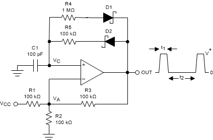
Figure 7-12 is a variation on the square wave oscillator that allows adjusting the pulse widths.
R4 and R5 provide separate charge and discharge paths for the capacitor C depending on the output state.
 Figure 7-12 Adjustable Pulse Width Generator
The charge path is set through R5 and D2 when the output is high. Similarly, the discharge path for the capacitor is set by R4 and D1 when the output is low.
The pulse width t1 is determined by the RC time constant of R5 and C. Thus, the time t2 between the pulses can be changed by varying R4, and the pulse width can be altered by R5. The frequency of the output can be changed by varying both R4 and R5. At low voltages, the effects of the diode forward drop (0.8 V, or 0.15 V for Shottky) must be taken into account by altering output high and low voltages in the calculations. RPU should be at least 10x less than the smallest value of R4 or R5.