SNOSDA4D June   2020  – November 2023 LM339LV , LM393LV , TL331LV , TL391LV

PRODMIX  

  1.   1
  2. Features
  3. Applications
  4. Description
  5. Pin Configuration and Functions
    1. 4.1 Pin Functions for TL331LV and TL391LV
    2. 4.2 Pin Functions: LM393LV
    3. 4.3 Pin Functions: LM339LV
  6. Specifications
    1. 5.1  Absolute Maximum Ratings
    2. 5.2  ESD Ratings
    3. 5.3  Recommended Operating Conditions
    4. 5.4  Thermal Information for TL3x1LV
    5. 5.5  Thermal Information, LM393LV
    6. 5.6  Thermal Information, LM339LV
    7. 5.7  Electrical Characteristics, TL3x1LV
    8. 5.8  Switching Characteristics, TL3x1LV
    9. 5.9  Electrical Characteristics, LM393LV
    10. 5.10 Switching Characteristics, LM393LV
    11. 5.11 Electrical Characteristics, LM339LV
    12. 5.12 Switching Characteristics, LM339LV
    13. 5.13 Typical Characteristics
  7. Detailed Description
    1. 6.1 Overview
    2. 6.2 Functional Block Diagram
    3. 6.3 Feature Description
    4. 6.4 Device Functional Modes
      1. 6.4.1 Open Drain Output
      2. 6.4.2 Power-On-Reset (POR)
      3. 6.4.3 Inputs
        1. 6.4.3.1 Rail to Rail Input
        2. 6.4.3.2 Fault Tolerant Inputs
        3. 6.4.3.3 Input Protection
      4. 6.4.4 ESD Protection
      5. 6.4.5 Unused Inputs
      6. 6.4.6 Hysteresis
  8. Application and Implementation
    1. 7.1 Application Information
      1. 7.1.1 Basic Comparator Definitions
        1. 7.1.1.1 Operation
        2. 7.1.1.2 Propagation Delay
        3. 7.1.1.3 Overdrive Voltage
      2. 7.1.2 Hysteresis
        1. 7.1.2.1 Inverting Comparator With Hysteresis
        2. 7.1.2.2 Non-Inverting Comparator With Hysteresis
    2. 7.2 Typical Applications
      1. 7.2.1 Window Comparator
        1. 7.2.1.1 Design Requirements
        2. 7.2.1.2 Detailed Design Procedure
        3. 7.2.1.3 Application Curve
      2. 7.2.2 Square-Wave Oscillator
        1. 7.2.2.1 Design Requirements
        2. 7.2.2.2 Detailed Design Procedure
        3. 7.2.2.3 Application Curve
      3. 7.2.3 Adjustable Pulse Width Generator
      4. 7.2.4 Time Delay Generator
      5. 7.2.5 Logic Level Shifter
      6. 7.2.6 One-Shot Multivibrator
      7. 7.2.7 Bi-Stable Multivibrator
      8. 7.2.8 Zero Crossing Detector
      9. 7.2.9 Pulse Slicer
    3. 7.3 Power Supply Recommendations
    4. 7.4 Layout
      1. 7.4.1 Layout Guidelines
      2. 7.4.2 Layout Example
  9. Device and Documentation Support
    1. 8.1 Related Documentation
    2. 8.2 Receiving Notification of Documentation Updates
    3. 8.3 Support Resources
    4. 8.4 Trademarks
    5. 8.5 Electrostatic Discharge Caution
    6. 8.6 Glossary
  10. Revision History
  11. 10Mechanical, Packaging, and Orderable Information

Package Options

Mechanical Data (Package|Pins)
Thermal pad, mechanical data (Package|Pins)
Orderable Information

One-Shot Multivibrator

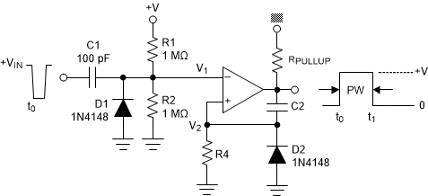
GUID-E0F7B693-4D06-4274-8ED6-7558B23F3A64-low.gifFigure 7-15 One-Shot Multivibrator

A monostable multivibrator has one stable state in which it can remain indefinitely. It can be triggered externally to another quasi-stable state. A monostable multivibrator can thus be used to generate a pulse of desired width.

The desired pulse width is set by adjusting the values of C2 and R4. The resistor divider of R1 and R2 can be used to determine the magnitude of the input trigger pulse. The output will change state when V1 < V2. Diode D2 provides a rapid discharge path for capacitor C2 to reset at the end of the pulse. The diode also prevents the non-inverting input from being driven below ground.