SNOS455G May 2000 – September 2015 LM4050-N , LM4050-N-Q1
PRODUCTION DATA.
- 1 Features
- 2 Applications
- 3 Description
- 4 Revision History
- 5 Pin Configuration and Functions
-
6 Specifications
- 6.1 Absolute Maximum Ratings
- 6.2 ESD Ratings
- 6.3 Recommended Operating Conditions
- 6.4 Thermal Information
- 6.5 Electrical Characteristics: 2-V Option
- 6.6 Electrical Characteristics: 2.5-V Option
- 6.7 Electrical Characteristics: 4.1-V Option
- 6.8 Electrical Characteristics: 5-V Option
- 6.9 Electrical Characteristics: 8.2-V Option
- 6.10 Electrical Characteristics: 10-V Option
- 6.11 Typical Characteristics
- 7 Parameter Measurement Information
- 8 Detailed Description
- 9 Application and Implementation
- 10Power Supply Recommendations
- 11Layout
- 12Device and Documentation Support
- 13Mechanical, Packaging, and Orderable Information
Package Options
Mechanical Data (Package|Pins)
- DBZ|3
Thermal pad, mechanical data (Package|Pins)
Orderable Information
8 Detailed Description
8.1 Overview
The LM4050-N device is a precision micropower shunt voltage reference. The part comes in 6 different fixed-output voltage options for space-constrained applications, removing the need for feedback resistors. The voltage tolerance accuracies are ±0.1%, ±0.2%, and ±0.5% for Versions A, B, and C, respectively. The LM4050-N comes in two application versions, Industrial and Extended temperature range, which are operational from –40°C to 85°C and –40°C to 125°C, respectively.
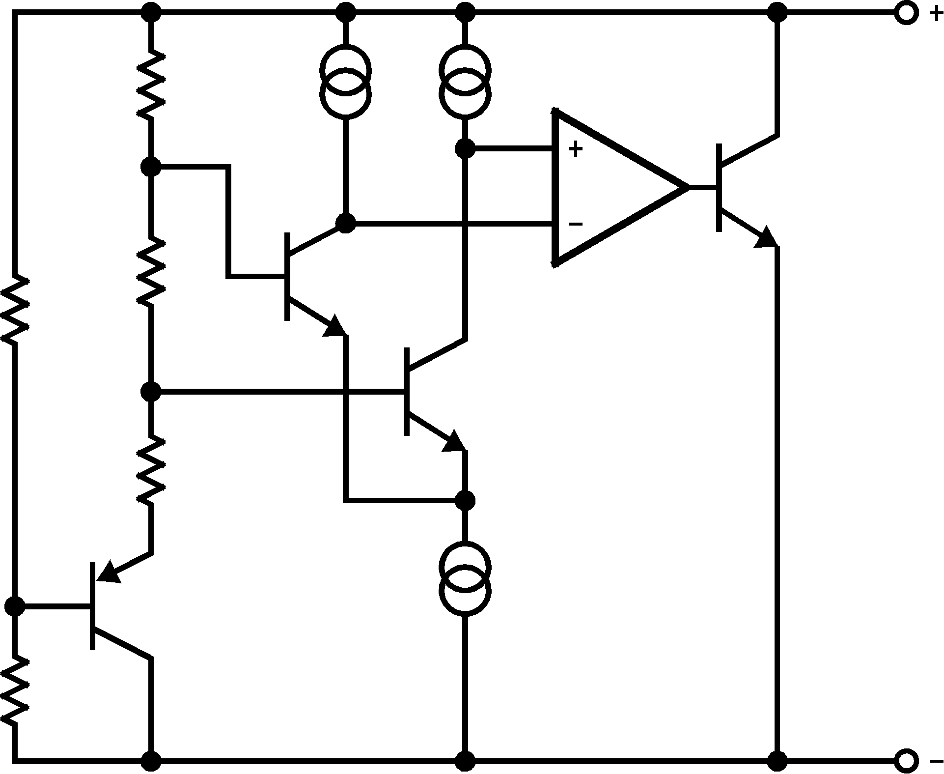
8.2 Functional Block Diagram

8.3 Feature Description
The LM4050-N behaves as a high-precision Zener diode. The voltage is regulated between its cathode and anode which is dependent on the current being supplied to the cathode. This current is needed for the LM4050-N to regulate within the specified limits. Refer to the minimum and maximum operating requirements for the specific voltage option used. The LM4050-N is internally compensated to be stable without the use of an output capacitor. However, if desired, a bypass capacitor may be used.
8.4 Device Functional Modes
The LM4050-N can only operate in closed loop due to the fact that the feedback resistors are internal to the device. Additionally, the output voltage cannot be adjusted for the same reason. The output voltage is regulated in a closed loop, provided the Rs (see Functional Block Diagram) resistor is sized to deliver the current to the cathode within the limits specified for the fixed-voltage version being used.