SNVSCA9 October 2022 LM5012
PRODUCTION DATA
- 1 Features
- 2 Applications
- 3 Description
- 4 Revision History
- 5 Device Comparison Table
- 6 Pin Configuration and Functions
- 7 Specifications
-
8 Detailed Description
- 8.1 Overview
- 8.2 Functional Block Diagram
- 8.3
Feature Description
- 8.3.1 Control Architecture
- 8.3.2 Internal VCC Regulator and Bootstrap Capacitor
- 8.3.3 Regulation Comparator
- 8.3.4 Internal Soft Start
- 8.3.5 On-Time Generator
- 8.3.6 Current Limit
- 8.3.7 N-Channel Buck Switch and Driver
- 8.3.8 Schottky Diode Selection
- 8.3.9 Enable and Undervoltage Lockout (EN/UVLO)
- 8.3.10 Power Good (PGOOD)
- 8.3.11 Thermal Protection
- 8.4 Device Functional Modes
- 9 Application and Implementation
- 10Device and Documentation Support
- 11Mechanical, Packaging, and Orderable Information
Package Options
Mechanical Data (Package|Pins)
- DDA|8
Thermal pad, mechanical data (Package|Pins)
- DDA|8
Orderable Information
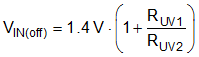
8.3.9 Enable and Undervoltage Lockout (EN/UVLO)
The LM5012 contains a dual-level EN/UVLO circuit. When the EN/UVLO voltage is below 1.1 V (typical), the converter is in a low-current shutdown mode and the input quiescent current (IQ) is dropped down to 3 µA. When the voltage is greater than 1.1 V but less than 1.5 V (typical), the converter is in standby mode. In standby mode, the internal bias regulator is active while the control circuit is disabled. When the voltage exceeds the rising threshold of 1.5 V (typical), normal operation begins. Install a resistor divider from VIN to GND to set the minimum operating voltage of the regulator. Use Equation 5 and Equation 6 to calculate the input UVLO turn-on and turn-off voltages, respectively.
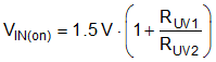
TI recommends selecting RUV1 in the range of 1 MΩ for most applications. A larger RUV1 consumes less DC current, which is mandatory if light-load efficiency is critical. If input UVLO is not required, the power-supply designer can either drive EN/UVLO as an enable input driven by a logic signal or connect it directly to VIN. If EN/UVLO is directly connected to VIN, the regulator begins switching as soon as the internal bias rails are active.