SNVS629F May 2011 – December 2019 LM5050-1 , LM5050-1-Q1
PRODUCTION DATA.
- 1 Features
- 2 Applications
- 3 Description
- 4 Revision History
- 5 Pin Configuration and Functions
- 6 Specifications
- 7 Detailed Description
-
8 Application and Implementation
- 8.1 Application Information
- 8.2
Typical Applications
- 8.2.1 Typical Application With Input and Output Transient Protection
- 8.2.2 Using a Separate VS Supply for Low Vin Operation
- 8.2.3 ORing of Two Power Sources
- 8.2.4 Reverse Input Voltage Protection With IQ Reduction
- 8.2.5 Basic Application With Input Transient Protection
- 8.2.6 48-V Application With Reverse Input Voltage (VIN = –48 V) Protection
- 9 Power Supply Recommendations
- 10Layout
- 11Device and Documentation Support
- 12Mechanical, Packaging, and Orderable Information
Package Options
Mechanical Data (Package|Pins)
- DDC|6
Thermal pad, mechanical data (Package|Pins)
Orderable Information
8.2.4 Reverse Input Voltage Protection With IQ Reduction
If Vs is powered while IN is floating or grounded, then about 0.5 mA will leak from the Vs pin into the IC and about 3 mA will leak from the OUT pin into the IC. From this leakage, about 50 uA will flow out of the IN pin and the rest will flow to ground. This does not affect long term reliability of the IC, but may influence circuit design.
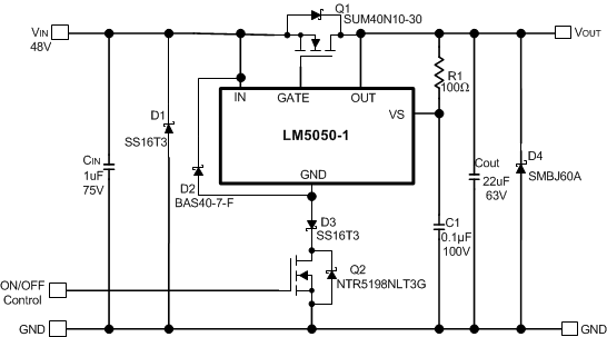
In battery powered applications, whenever LM5050-1 functionality is not needed, the supply to the LM5050-1 can be disconnected by turning “OFF” Q2, as shown in Figure 29. This disconnects the ground path of the LM5050-1 and eliminates the current leakage from the battery.
The quiescent current of LM5050-1 can be also reduced by disconnecting the supply to VS pin, whenever LM5050-1 function is not need.
 Figure 29. Reverse Input Voltage Protection With IQ Reduction Schematic