SNVS628H October 2009 – December 2019 LM5060
PRODUCTION DATA.
- 1 Features
- 2 Applications
- 3 Description
- 4 Revision History
- 5 Pin Configuration and Functions
- 6 Specifications
- 7 Detailed Description
-
8 Application and Implementation
- 8.1 Application Information
- 8.2
Typical Applications
- 8.2.1
Example Number 1: LM5060EVAL Design
- 8.2.1.1 Design Requirements
- 8.2.1.2
Detailed Design Procedure
- 8.2.1.2.1 VDS Fault Detection and Selecting Sense Pin Resistor RS
- 8.2.1.2.2 Turn-On Time
- 8.2.1.2.3 Fault Detection Delay Time
- 8.2.1.2.4 MOSFET Selection
- 8.2.1.2.5 Input and Output Capacitors
- 8.2.1.2.6 UVLO, OVP
- 8.2.1.2.7 POWER GOOD Indicator
- 8.2.1.2.8 Input Bypass Capacitor
- 8.2.1.2.9 Large Load Capacitance
- 8.2.1.3 Application Curves
- 8.2.2 Example Number 2: Reverse Polarity Protection With Diodes
- 8.2.3 Example Number 3: Reverse Polarity Protection With Resistor
- 8.2.1
Example Number 1: LM5060EVAL Design
- 9 Power Supply Recommendations
- 10Layout
- 11Device and Documentation Support
- 12Mechanical, Packaging, and Orderable Information
Package Options
Mechanical Data (Package|Pins)
- DGS|10
Thermal pad, mechanical data (Package|Pins)
Orderable Information
8.2.2 Example Number 2: Reverse Polarity Protection With Diodes
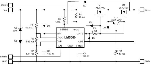
 Figure 39. Application with Reverse Polarity Protection with Diodes for OUT Pin Protection
 Figure 39 shows the LM5060 in an automotive application with reverse polarity protection. The second N-channel MOSFET Q2 is used to prevent the body diode of Q1 from conducting in a reverse VIN polarity situation. The zener diode D3 is used to limit VIN voltage transients which will occur when Q1 and Q2 are shut off quickly. In some applications the inductive kick is handled by input capacitors and D3 can be omitted. In reverse polarity protected applications, the input capacitors will see the reverse voltage. To avoid stressing input capacitors with reverse polarity, a transorb circuit implemented with D3 and D2 may be used. Diode D1 in Figure 39 protects the VIN pin in the event of reverse polarity. The resistor R1 protects the GATE pin from reverse currents exceeding 25 mA in the reverse polarity situation. This GATE resistor would slow down the shutdown of Q1 and Q2 dramatically. To prevent a slow turn off in fault conditions, D5 is added to bypass the current limiting resistor R1. When Q1 and Q2 are turned on, R1 does not cause any delay because the GATE pin is driven with a 24-µA current source. D6, Q3 and R2 protect Q2 from VGS damage in the event of reverse input polarity. Diodes D5 and D7 are only necessary if the output load is highly capacitive. Such a capacitive load in combination with a high reverse polarity input voltage condition can exceed the power rating of the internal zener diode between OUT pin and GATE pin as well as the internal diode between the OUT pin and SENSE pin. External diodes D5 and D7 should be used in reverse polarity protected applications with large capacitive loads.