SNVS954H February 2013 – June 2017 LM5122
PRODUCTION DATA.
- 1 Features
- 2 Applications
- 3 Description
- 4 Revision History
- 5 Pin Configuration and Functions
- 6 Specifications
-
7 Detailed Description
- 7.1 Overview
- 7.2 Functional Block Diagram
- 7.3
Feature Description
- 7.3.1 Undervoltage Lockout (UVLO)
- 7.3.2 High Voltage VCC Regulator
- 7.3.3 Oscillator
- 7.3.4 Slope Compensation
- 7.3.5 Error Amplifier
- 7.3.6 PWM Comparator
- 7.3.7 Soft-Start
- 7.3.8 HO and LO Drivers
- 7.3.9 Bypass Operation (VOUT = VIN)
- 7.3.10 Cycle-by-Cycle Current Limit
- 7.3.11 Clock Synchronization
- 7.3.12 Maximum Duty Cycle
- 7.3.13 Thermal Protection
- 7.4 Device Functional Modes
-
8 Application and Implementation
- 8.1
Application Information
- 8.1.1 Feedback Compensation
- 8.1.2 Sub-Harmonic Oscillation
- 8.1.3 Interleaved Boost Configuration
- 8.1.4 DCR Sensing
- 8.1.5 Output Overvoltage Protection
- 8.1.6 SEPIC Converter Simplified Schematic
- 8.1.7 Non-Isolated Synchronous Flyback Converter Simplified Schematic
- 8.1.8 Negative to Positive Conversion
- 8.2
Typical Application
- 8.2.1 Design Requirements
- 8.2.2
Detailed Design Procedure
- 8.2.2.1 Custom Design With WEBENCH® Tools
- 8.2.2.2 Timing Resistor RT
- 8.2.2.3 UVLO Divider RUV2, RUV1
- 8.2.2.4 Input Inductor LIN
- 8.2.2.5 Current Sense Resistor RS
- 8.2.2.6 Current Sense Filter RCSFP, RCSFN, CCS
- 8.2.2.7 Slope Compensation Resistor RSLOPE
- 8.2.2.8 Output Capacitor COUT
- 8.2.2.9 Input Capacitor CIN
- 8.2.2.10 VIN Filter RVIN, CVIN
- 8.2.2.11 Bootstrap Capacitor CBST and Boost Diode DBST
- 8.2.2.12 VCC Capacitor CVCC
- 8.2.2.13 Output Voltage Divider RFB1, RFB2
- 8.2.2.14 Soft-Start Capacitor CSS
- 8.2.2.15 Restart Capacitor CRES
- 8.2.2.16 Low-Side Power Switch QL
- 8.2.2.17 High-Side Power Switch QH and Additional Parallel Schottky Diode
- 8.2.2.18 Snubber Components
- 8.2.2.19 Loop Compensation Components CCOMP, RCOMP, CHF
- 8.2.3 Application Curves
- 8.1
Application Information
- 9 Power Supply Recommendations
- 10Layout
- 11Device and Documentation Support
- 12Mechanical, Packaging, and Orderable Information
Package Options
Mechanical Data (Package|Pins)
Thermal pad, mechanical data (Package|Pins)
Orderable Information
7 Detailed Description
7.1 Overview
The LM5122 wide input range synchronous boost controller features all of the functions necessary to implement a highly efficient synchronous boost regulator. The regulator control method is based upon peak current mode control. Peak current mode control provides inherent line feedforward and ease of loop compensation. This highly integrated controller provides strong high-side and low-side N-channel MOSFET drivers with adaptive dead-time control. The switching frequency is user programmable up to 1 MHz set by a single resistor or synchronized to an external clock. The 180º-shifted clock output of the LM5122 enables easy multi-phase configuration.
The control mode of high-side synchronous switch can be configured as either forced PWM (FPWM) or diode-emulation mode. Fault protection features include cycle-by-cycle current limiting, hiccup mode over load protection, thermal shutdown and remote shutdown capability by pulling down the UVLO pin. The UVLO input enables the controller when the input voltage reaches a user selected threshold, and provides a tiny 9-μA shutdown quiescent current when pulled low. The device is available in a 20 and 24-pin HTSSOP package featuring an exposed pad to aid in thermal dissipation.
7.2 Functional Block Diagram
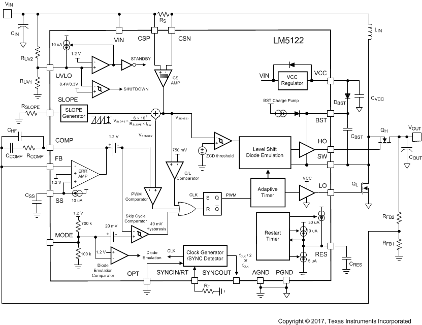
7.3 Feature Description
7.3.1 Undervoltage Lockout (UVLO)
The LM5122 features a dual level UVLO circuit. When the UVLO pin voltage is less than the 0.4-V UVLO standby enable threshold, the LM5122 is in the shutdown mode with all functions disabled. The shutdown comparator provides 0.1 V of hysteresis to avoid chatter during transition. If the UVLO pin voltage is greater than 0.4 V and below 1.2 V during power up, the controller is in standby mode with the VCC regulator operational and no switching at the HO and LO outputs. This feature allows the UVLO pin to be used as a remote shutdown function by pulling the UVLO pin down below the UVLO standby enable threshold with an external open collector or open drain device.
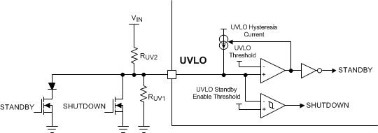 Figure 16. UVLO Remote Standby and Shutdown Control
If the UVLO pin voltage is above the 1.2-V UVLO threshold and VCC voltage exceeds the VCC UV threshold, a startup sequence begins. UVLO hysteresis is accomplished with an internal 10-μA current source that is switched on or off into the impedance of the UVLO setpoint divider. When the UVLO pin voltage exceeds 1.2 V, the current source is enabled to quickly raise the voltage at the UVLO pin. When the UVLO pin voltage falls below the 1.2-V UVLO threshold, the current source is disabled causing the voltage at the UVLO pin to quickly fall. In addition to the UVLO hysteresis current source, a 5-μs deglitch filter on both rising and falling edge of UVLO toggling helps preventing chatter upon power up or down.
An external UVLO setpoint voltage divider from the supply voltage to AGND is used to set the minimum input operating voltage of the regulator. The divider must be designed such that the voltage at the UVLO pin is greater than 1.2 V when the input voltage is in the desired operating range. The maximum voltage rating of the UVLO pin is 15 V. If necessary, the UVLO pin can be clamped with an external zener diode. The UVLO pin should not be left floating. The values of RUV1 and RUV2 can be determined from Equation 1 and Equation 2.


where
- VHYS is the desired UVLO hysteresis
- VIN(STARTUP) is the desired startup voltage of the regulator during turn-on.
Typical shutdown voltage during turn-off can be calculated as follows:

7.3.2 High Voltage VCC Regulator
The LM5122 contains an internal high voltage regulator that provides typical 7.6 V VCC bias supply for the controller and N-channel MOSFET drivers. The input of VCC regulator, VIN, can be connected to an input voltage source as high as 65 V. The VCC regulator turns on when the UVLO pin voltage is greater than 0.4 V. When the input voltage is below the VCC setpoint level, the VCC output tracks VIN with a small dropout voltage. The output of the VCC regulator is current limited at 50 mA minimum.
Upon power-up, the VCC regulator sources current into the capacitor connected to the VCC pin. TI recommends a capacitance range for the VCC capacitor of 1 μF to 47 μF, and capacitance is recommended to be at least 10 times greater than CBST value. When operating with a VIN voltage less than 6 V, the value of VCC capacitor must be 4.7 µF or greater.
The internal power dissipation of the LM5122 device can be reduced by supplying VCC from an external supply. If an external VCC bias supply exists and the voltage is greater than 9 V and below 14.5 V. The external VCC bias supply can be applied to the VCC pin directly through a diode, as shown in Figure 17.
 Figure 17. External Bias Supply when 9 V < VEXT< 14.5 V
Shown in Figure 18 is a method to derive the VCC bias voltage with an additional winding on the boost inductor. This circuit must be designed to raise the VCC voltage above VCC regulation voltage to shut off the internal VCC regulator.
 Figure 18. External Bias Supply using Transformer
The VCC regulator series pass transistor includes a diode between VCC and VIN that must not be fully forward biased in normal operation, as shown in Figure 19. If the voltage of the external VCC bias supply is greater than the VIN pin voltage, an external blocking diode is required from the input power supply to the VIN pin to prevent the external bias supply from passing current to the input supply through VCC. The need for the blocking diode should be evaluated for all applications when the VCC is supplied by the external bias supply. Especially, when the input power supply voltage is less than 4.5 V, the external VCC supply should be provided and the external blocking diode is required.
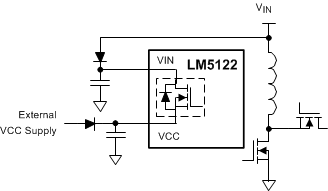 Figure 19. VIN Configuration when VVIN < VVCC
7.3.3 Oscillator
The LM5122 switching frequency is programmable by a single external resistor connected between the RT pin and the AGND pin. The resistor should be located very close to the device and connected directly to the RT pin and AGND pin. To set a desired switching frequency (fSW), the resistor value can be calculated from Equation 4.

7.3.4 Slope Compensation
For duty cycles greater than 50%, peak current mode regulators are subject to sub-harmonic oscillation. Sub-harmonic oscillation is normally characterized by observing alternating wide and narrow duty cycles. This sub-harmonic oscillation can be eliminated by a technique, which adds an artificial ramp, known as slope compensation, to the sensed inductor current.
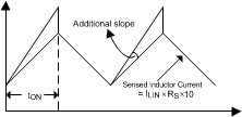 Figure 20. Slope Compensation
The amount of slope compensation is programmable by a single resistor connected between the SLOPE pin and the AGND pin. The amount of slope compensation can be calculated as follows:

where
RSLOPE value can be determined from Equation 6 at minimum input voltage:

where
- K=0.82~1 as a default
From Equation 6, K can be calculated over the input range as follows:

where
In any case, K should be greater than at least 0.5. At higher switching frequency over 500 kHz, K factor is recommended to be greater than or equal to 1 because the minimum on-time affects the amount of slope compensation due to internal delays.
The sum of sensed inductor current and slope compensation should be less than COMP output high voltage (VOH) for proper startup with load and proper current limit operation. This limits the minimum value of RSLOPE to be:

where
- This equation can be used in most cases
- Consider this conservative selection when VIN(MIN) < 5.5 V

where
The SLOPE pin cannot be left floating.
7.3.5 Error Amplifier
The internal high-gain error amplifier generates an error signal proportional to the difference between the FB pin voltage and the internal precision 1.2-V reference. The output of the error amplifier is connected to the COMP pin allowing the user to provide a Type 2 loop compensation network.
RCOMP, CCOMP and CHF configure the error amplifier gain and phase characteristics to achieve a stable voltage loop. This network creates a pole at DC, a mid-band zero (fZ_EA) for phase boost, and a high frequency pole (fP_EA). The minimum recommended value of RCOMP is 2 kΩ. See the Feedback Compensation section.


7.3.6 PWM Comparator
The PWM comparator compares the sum of sensed inductor current and slope compensation ramp to the voltage at the COMP pin through a 1.2-V internal COMP to PWM voltage drop, and terminates the present cycle when the sum of sensed inductor current and slope compensation ramp is greater than VCOMP –1.2 V.
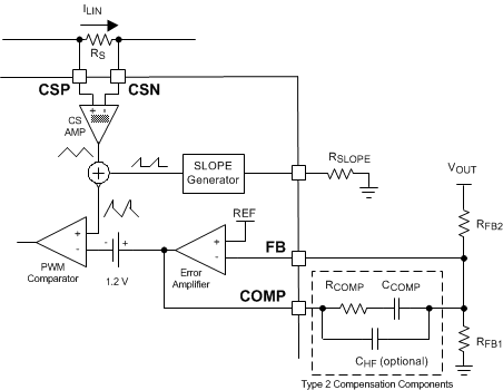 Figure 21. Feedback Configuration and PWM Comparator
7.3.7 Soft-Start
The soft-start feature helps the regulator to gradually reach the steady state operating point, thus reducing start-up stresses and surges. The LM5122 regulates the FB pin to the SS pin voltage or the internal 1.2-V reference, whichever is lower. The internal 10-μA soft-start current source gradually increases the voltage on an external soft-start capacitor connected to the SS pin. This results in a gradual rise of the output voltage starting from the input voltage level to the target output voltage. Soft-start time (tSS) which varies by the input supply voltage and is calculated from Equation 11.

When the UVLO pin voltage is greater than the 1.2-V UVLO threshold and VCC voltage exceeds the VCC UV threshold, an internal 10-μA soft-start current source turns on. At the beginning of this soft-start sequence, allow VSS to fall down below 25 mV using the internal SS pulldown switch. The SS pin can be pulled down by external switch to stop switching, but pulling up to enable switching is not allowed. The start-up delay (see Figure 22) must be long enough for high-side boot capacitor to be fully charged up by internal BST charge pump.
The value of CSS must be large enough to charge the output capacitor during soft-start time.

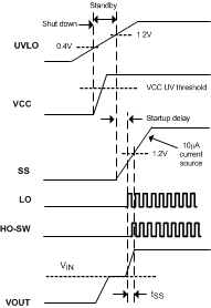 Figure 22. Startup Sequence
7.3.8 HO and LO Drivers
The LM5122 contains strong N-channel MOSFET gate drivers and an associated high-side level shifter to drive the external N-channel MOSFET switches. The high-side gate driver works in conjunction with an external boot diode DBST, and bootstrap capacitor CBST. During the on-time of the low-side N-channel MOSFET driver, the SW pin voltage is approximately 0 V and the CBST is charged from VCC through the DBST. TI recommends a 0.1-μF or larger ceramic capacitor, connected with short traces between the BST and SW pin.
The LO and HO outputs are controlled with an adaptive dead-time methodology which insures that both outputs are never enabled at the same time. When the controller commands LO to be enabled, the adaptive dead-time logic first disables HO and waits for HO-SW voltage to drop. LO is then enabled after a small delay (HO fall to LO rise delay). Similarly, the HO turnon is delayed until the LO voltage has discharged. HO is then enabled after a small delay (LO fall to HO rise delay). This technique insures adequate dead-time for any size N-channel MOSFET device, especially when VCC is supplied by a higher external voltage source. Be careful when adding series gate resistors, as this may decrease the effective dead-time.
Exercise care when selecting the N-channel MOSFET devices threshold voltage, especially if the VIN voltage range is below the VCC regulation level or a bypass operation is required. If the bypass operation is required, especially when output voltage is less than 12 V, a logic level device should be selected for the high-side N-channel MOSFET. During start-up at low input voltages, the low-side N-channel MOSFET switch’s gate plateau voltage must be sufficient to completely enhance the N-channel MOSFET device. If the low-side N-channel MOSFET drive voltage is lower than the low-side N-channel MOSFET device gate plateau voltage during startup, the regulator may not start up properly and it may stick at the maximum duty cycle in a high power dissipation state. This condition can be avoided by selecting a lower threshold N-channel MOSFET switch or by increasing VIN(STARTUP) with the UVLO pin voltage programming.
7.3.9 Bypass Operation (VOUT = VIN)
The LM5122 allows 100% duty cycle operation for the high-side synchronous switch when the input supply voltage is equal to or greater than the target output voltage. An internal 200 μA BST charge pump maintains sufficient high-side driver supply voltage to keep the high-side N-channel MOSFET switch on without the power stage switching. The internal BST charge pump is enabled when the UVLO pin voltage is greater than 1.2 V and the VCC voltage exceeds the VCC UV threshold. The BST charge pump generates 5.3-V minimum BST to SW voltage when SW voltage is greater than 9 V. This requires minimum 9 V boost output voltage for proper bypass operation. The leakage current of the boot diode should be always less than the BST charge pump sourcing current to maintain a sufficient driver supply voltage at both low and high temperatures. Forced-PWM mode is the recommended PWM configuration when bypass operation is required.
7.3.10 Cycle-by-Cycle Current Limit
The LM5122 features a peak cycle-by-cycle current limit function. If the CSP to CSN voltage exceeds the 75-mV cycle-by-cycle current limit threshold, the current limit comparator immediately terminates the LO output.
For the case where the inductor current may overshoot, such as inductor saturation, the current limit comparator skips pulses until the current has decayed below the current limit threshold. Peak inductor current in current limit can be calculated as follows:

7.3.11 Clock Synchronization
The SYNCIN/RT pin can be used to synchronize the internal oscillator to an external clock. A positive going synchronization clock at the RT pin must exceed the RT sync rising threshold and negative going synchronization clock at RT pin must exceed the RT sync falling threshold to trip the internal synchronization pulse detector.
In Master1 mode, two types of configurations are allowed for clock synchronization. With the configuration in Figure 23, the frequency of the external synchronization pulse is recommended to be within +40% and –20% of the internal oscillator frequency programmed by the RT resistor. For example, 900-kHz external synchronization clock and 20-kΩ RT resistor are required for 450-kHz switching in master1 mode. The internal oscillator can be synchronized by AC coupling a positive edge into the RT pin. A 5-V amplitude pulse signal coupled through 100-pF capacitor is a good starting point. The RT resistor is always required with AC coupling capacitor with the Figure 23 configuration, whether the oscillator is free running or externally synchronized.
Care should be taken to ensure that the RT pin voltage does not go below –0.3 V at the falling edge of the external pulse. This may limit the duty cycle of external synchronization pulse. There is approximately 400-ns delay from the rising edge of the external pulse to the rising edge of LO.
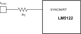 Figure 23. Oscillator Synchronization Through AC Coupling in Master1 Mode
With the configuration in Figure 24, the internal oscillator can be synchronized by connecting the external synchronization clock into the RT pin through RT resistor with free of the duty cycle limit. The output stage of the external clock source should be a low impedance totem-pole structure. Default logic state of fSYNC must be low.
 Figure 24. Oscillator Synchronization Through a Resistor in Master1 Mode
In master2 and slave modes, this external synchronization clock should be directly connected to the RT pin and always provided continuously. The internal oscillator frequency can be either of two times faster than switching frequency or the same as the switching frequency by configuring the combination of FB and OPT pins (see Table 1).
7.3.12 Maximum Duty Cycle
When operating with a high PWM duty cycle, the low-side N-channel MOSFET device is forced off each cycle. This forced LO off-time limits the maximum duty cycle of the controller. When designing a boost regulator with high switching frequency and high duty-cycle requirements, check the required maximum duty cycle. The minimum input supply voltage that can achieve the target output voltage is estimated from Equation 14 or Equation 15.
Use Equation 14 if VVCC is greater than 5.5 V or VVIN is greater than 6 V. For low voltage applications that do not satisfy either of these conditions use Equation 15.

In normal operation, about 100 ns of margin is recommended.
7.3.13 Thermal Protection
Internal thermal shutdown circuitry is provided to protect the controller in the event the maximum junction temperature is exceeded. When activated, typically at 165°C, the controller is forced into a low-power shutdown mode, disabling the output drivers, disconnection switch and the VCC regulator. This feature is designed to prevent overheating and destroying the device.
7.4 Device Functional Modes
7.4.1 MODE Control (Forced-PWM Mode and Diode-Emulation Mode)
A fully synchronous boost regulator implemented with a high-side switch rather than a diode has the capability to sink current from the output in certain conditions such as light load, overvoltage or load transient. The LM5122 can be configured to operate in either forced-PWM mode (FPWM) or diode emulation mode.
In FPWM, reverse current flow in high-side N-channel MOSFET switch is allowed, and the inductor current conducts continuously at light or no load conditions. The benefit of the forced PWM mode is fast light load to heavy load transient response and constant frequency operation at light or no load conditions. To enable FPWM, connect the MODE pin to VCC or tie to a voltage greater than 1.2 V. In FPWM, reverse current flow is not limited.
In diode-emulation mode, current flow in the high-side switch is only permitted in one direction (source to drain). Turnon of the high-side switch is allowed if CSP to CSN voltage is greater than 7 mV rising threshold of zero current detection during low-side switch on-time. If CSP to CSN voltage is less than 6-mV falling threshold of zero current detection during high-side switch on-time, reverse current flow from output to input through the high-side N-channel MOSFET switch is prevented and discontinuous conduction mode of operation is enabled by latching off the high-side N-channel MOSFET switch for the remainder of the PWM cycle. A benefit of the diode emulation is lower power loss at light load conditions.
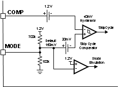 Figure 25. MODE Selection
During start-up the LM5122 forces diode emulation, for start-up into a pre-biased load, while the SS pin voltage is less than 1.2 V. Forced diode emulation is terminated by a pulse from PWM comparator when SS is greater than 1.2 V. If there are no LO pulses during the soft-start period, a 350-ns one-shot LO pulse is forced at the end of soft start to help charge the boot strap capacitor. Due to the internal current sense delay, configuring the LM5122 for diode emulation mode must be carefully evaluated if the inductor current ripple ratio is high and when operating at very high switching frequency. The transient performance during full load to no load in FPWM mode should also be verified.
7.4.2 MODE Control (Skip-Cycle Mode and Pulse-Skipping Mode)
Light load efficiency of the regulator typically drops as the losses associated with switching and bias currents of the converter become a significant percentage of the total power delivered to the load. In order to increase the light load efficiency the LM5122 provides two types of light load operation in diode-emulation mode.
The skip-cycle mode integrated into the LM5122 controller reduces switching losses and improves efficiency at light-load condition by reducing the average switching frequency. Skip-cycle operation is achieved by the skip cycle comparator. When a light-load condition occurs, the COMP pin voltage naturally decreases, reducing the peak current delivered by the regulator. During COMP voltage falling, the skip-cycle threshold is defined as VMODE –20 mV and during COMP voltage rising, it is defined as VMODE +20 mV. There is 40mV of internal hysteresis in the skip cycle comparator.
When the voltage at PWM comparator input falls below VMODE –20 mV, both HO and LO outputs are disabled. The controller continues to skip switching cycles until the voltage at PWM comparator input increases to VMODE + 20 mV, demanding more inductor current. The number of cycles skipped depends upon the load and the response time of the frequency compensation network. The internal hysteresis of skip-cycle comparator helps to produce a long skip cycle interval followed by a short burst of pulses. An internal 700-kΩ pullup and 100-kΩ pulldown resistor sets the MODE pin to 0.15 V as a default. Because the peak current limit threshold is set to 750 mV, the default skip threshold corresponds to approximately 17% of the peak level. In practice the skip level is lower due to the added slope compensation. By adding an external pullup resistor to SLOPE or VCC pin or adding an external pulldown resistor to the ground, the skip cycle threshold can be programmed. Because the skip cycle comparator monitors the PWM comparator input which is proportional to the COMP voltage, skip-cycle operation is not recommended when the bypass operation is required.
Conventional pulse-skipping operation can be achieved by connecting the MODE pin to ground. The negative 20-mV offset at the positive input of skip-cycle comparator ensures the skip-cycle comparator does not trigger in normal operation. At light or no load conditions, the LM5122 skips LO pulses if the pulse width required by the regulator is less than the minimum LO on-time of the device. Pulse skipping appears as a random behavior as the error amplifier struggles to find an average pulse width for LO in order to maintain regulation at light or no load conditions.
7.4.3 Hiccup-Mode Overload Protection
If cycle-by-cycle current limit is reached during any cycle, a 30-μA current is sourced into the RES capacitor for the remainder of the clock cycle. If the RES capacitor voltage exceeds the 1.2-V restart threshold, a hiccup mode over load protection sequence is initiated; The SS capacitor is discharged to GND, both LO and HO outputs are disabled, the voltage on the RES capacitor is ramped up and down between 2-V hiccup counter lower threshold and 4-V hiccup counter upper threshold eight times by 10-μA charge and 5-μA discharge currents. After the eighth cycles, the SS capacitor is released and charged by the 10-μA soft-start current again. If a 3-V zener diode is connected in parallel with the RES capacitor, the regulator enters into the hiccup-mode off mode and then never restarts until UVLO shutdown is cycled. Connect RES pin directly to the AGND when the hiccup-mode operation is not used.
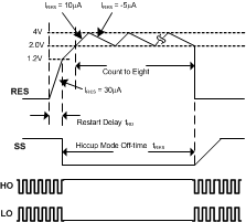 Figure 26. Hiccup Mode Overload Protection
7.4.4 Slave Mode and SYNCOUT
The LM5122 is designed to easily implement dual (or higher) phase boost converters by configuring one controller as a master and all others as slaves. Slave mode is activated by connecting the FB pin to the VCC pin. The FB pin is sampled during initial power-on and if a slave configuration is detected, the state is latched. In the slave mode, the error amplifier is disabled and has a high impedance output, 10-μA hiccup-mode off-time charging current and 5-μA hiccup-mode off-time discharging current are disabled, 5-μA normal-state RES discharging current and 10-μA soft-start charging current are disabled, 30 μA fault-state RES charging current is changed to 35 μA. 10-μA UVLO hysteresis current source works the same as master mode. Also, in slave mode, the internal oscillator is disabled, and an external synchronization clock is required.
The SYNCOUT function provides a 180° phase shifted clock output, enabling easy dual-phase interleaved configuration. By directly connecting master1 SYNCOUT to slave1 SYNCIN, the switching frequency of slave controller is synchronized to the master controller with 180º phase shift. In master mode, if OPT pin is tied to GND, an internal oscillator clock divided by two with 50% duty cycle is provided to achieve an 180º phase-shifted operation in two phase interleaved configuration. Switching frequency of master controller is half of the external clock frequency with this configuration. If the OPT pin voltage is higher than 2.7-V OPT threshold or the pin is tied to VCC, SYNCOUT is disabled and the switching frequency of master controller becomes the same as the external clock frequency. An external synchronization clock should be always provided and directly connected to SYNCIN for master2, slave1 and slave2 configurations. See Interleaved Boost Configuration for detailed information.
Table 1. LM5122 Multiphase Configuration
| MULTIPHASE CONFIGURATION | FB | OPT | ERROR AMPLIFIER | SWITCHING FREQUENCY | SYNCOUT |
|---|---|---|---|---|---|
| Master1 | Feedback | GND | Enable | fSYNC/2, Free running with RT resistor | fSYNC/2, fSW –180º |
| Slave1 | VCC | GND | Disable | fSYNC, No free running | Disable |
| Master2 | Feedback | VCC | Enable | fSYNC, No free running | Disable |
| Slave2 | VCC | VCC | Disable | fSYNC/2, No free running | fSYNC/2, fSW –180º |


