SLVSES8A October 2020 – December 2020 LM5127-Q1
PRODUCTION DATA
- 1 Features
- 2 Applications
- 3 Description
- 4 Revision History
- 5 Description (continued)
- 6 Pin Configuration and Functions
- 7 Specifications
-
8 Detailed Description
- 8.1 Overview
- 8.2 Functional Block Diagram
- 8.3
Feature Description
- 8.3.1 Device Enable (EN, VCC_HOLD)
- 8.3.2 Dual Input VCC Regulator (BIAS, VCCX, VCC)
- 8.3.3 Dual Input VDD Switch (VDD, VDDX)
- 8.3.4 Device Configuration and Light Load Switching Mode Selection (CFG/MODE)
- 8.3.5 Fixed or Adjustable Output Regulation Target (VOUT, FB)
- 8.3.6 Overvoltage Protection (VOUT, FB)
- 8.3.7 Power Good Indicator (PGOOD)
- 8.3.8 Programmable Switching Frequency (RT)
- 8.3.9 External Clock Synchronization (SYNC)
- 8.3.10 Programmable Spread Spectrum (DITHER)
- 8.3.11 Programmable Soft Start (SS)
- 8.3.12 Fast Re-start using VCC_HOLD (VCC_HOLD)
- 8.3.13 Transconductance Error Amplifier and PWM (COMP)
- 8.3.14 Current Sensing and Slope Compensation (CSA, CSB)
- 8.3.15 Constant Peak Current Limit (CSA, CSB)
- 8.3.16 Maximum Duty Cycle and Minimum Controllable On-time Limits (Boost)
- 8.3.17 Bypass Mode (Boost)
- 8.3.18 Minimum Controllable On-time and Minimum Controllable Off-time Limits (Buck)
- 8.3.19 Low Dropout Mode for Extended Minimum Input Voltage (Buck)
- 8.3.20 Programmable Hiccup Mode Overload Protection (RES)
- 8.3.21 MOSFET Drivers and Hiccup Mode Fault Protection (LO, HO, HB)
- 8.3.22 Battery Monitor (BMOUT, BMIN_FIX, BMIN_PRG)
- 8.3.23 Dual-phase Interleaved Configuration for High Current Supply (CFG)
- 8.3.24 Thermal Shutdown Protection
- 8.3.25 External VCCX Supply Reduces Power Dissipation
- 8.4 Device Functional Modes
- 9 Application and Implementation
- 10Power Supply Recommendations
- 11Layout
- 12Device and Documentation Support
- 13Mechanical, Packaging, and Orderable Information
Package Options
Mechanical Data (Package|Pins)
- RGZ|48
Thermal pad, mechanical data (Package|Pins)
- RGZ|48
Orderable Information
8.3.21 MOSFET Drivers and Hiccup Mode Fault Protection (LO, HO, HB)
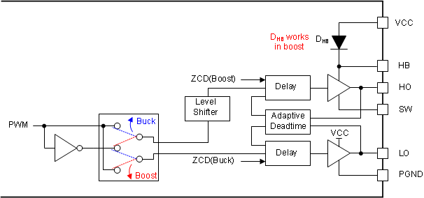
The device provides N-channel logic MOSFET drivers which can source a peak current of 2.2 A and sink a peak current of 3.3 A. The drivers are powered by VCC or HB, and enabled when EN is greater than VEN and VCC is greater than VVCC-UVLO.
When the low-side driver turns on, the SW pin voltage is approximately 0 V and the CHB is charged from VCC through a boot diode. In boost configuration, the boot diode is internally connected from VCC to HB1. Connect external boot diodes in buck configuration. The recommended minimum value of CHB is 0.1-μF.
The LO and HO outputs are controlled with an adaptive dead-time methodology which ensures that both outputs are not enabled at the same time. When the device commands LO to be enabled, the adaptive dead-time logic first disables HO and waits for HO-SW voltage to drop. LO is then enabled after a small delay. Similarly, the HO turnon is delayed until the LO-PGND voltage has discharged. HO is then enabled after a small delay. The adaptive dead-time circuit insures that both outputs are not enabled at the same time when QG@5V is less than 40 nC over the temperature.
If the minimum BIAS pin voltage is below VVCC-REG, extra care should be taken when selecting the MOSFETs. Especially during start-up at low BIAS input voltage, the gate plateau voltage of the MOSFET should be less than the BIAS pin voltage to completely enhance the MOSFET. If the driver output voltage is lower than the MOSFET gate plateau voltage during start-up, the converter may not start up properly and it can stick at the maximum duty cycle in a high power dissipation state. This condition can be avoided by selecting a lower threshold MOSFET or by turning on the channel when the BIAS pin voltage is sufficient.
 Figure 8-23 Driver Structure (Internal
boot diode is available only in boost)
Figure 8-23 Driver Structure (Internal
boot diode is available only in boost)The hiccup mode protection is triggered by the HB UVLO in boost configuration. If the HB-to-SW voltage is less than the HB UVLO threshold (VHB-UVLO), the LO turns on for 75 ns to replenish the boost capacitor. The device allows up to four consecutive replenish switchings. After four consecutive boot replenish switching, the channel skips the boot replenish switching for 12 cycles. If the channel fails to replenish the boost capacitor after the four sets of the four consecutive replenish switching, the channel stops switching and enters hiccup mode fault protection.
If required, the slew rate of the switching node voltage is adjusted by the resistor in series with the HB pin up to 5-Ω in buck configuration. If required, use a gate resistor in parallel with a pulldown PNP transistor. Care should be taken when adding a gate resistor as this can decrease the effective dead-time.
 Figure 8-24 Slew Rate Control (a) HB
Resistor for Buck, (b) Gate Resistor with Pulldown PNP Transistor