SLVSES8A October 2020 – December 2020 LM5127-Q1
PRODUCTION DATA
- 1 Features
- 2 Applications
- 3 Description
- 4 Revision History
- 5 Description (continued)
- 6 Pin Configuration and Functions
- 7 Specifications
-
8 Detailed Description
- 8.1 Overview
- 8.2 Functional Block Diagram
- 8.3
Feature Description
- 8.3.1 Device Enable (EN, VCC_HOLD)
- 8.3.2 Dual Input VCC Regulator (BIAS, VCCX, VCC)
- 8.3.3 Dual Input VDD Switch (VDD, VDDX)
- 8.3.4 Device Configuration and Light Load Switching Mode Selection (CFG/MODE)
- 8.3.5 Fixed or Adjustable Output Regulation Target (VOUT, FB)
- 8.3.6 Overvoltage Protection (VOUT, FB)
- 8.3.7 Power Good Indicator (PGOOD)
- 8.3.8 Programmable Switching Frequency (RT)
- 8.3.9 External Clock Synchronization (SYNC)
- 8.3.10 Programmable Spread Spectrum (DITHER)
- 8.3.11 Programmable Soft Start (SS)
- 8.3.12 Fast Re-start using VCC_HOLD (VCC_HOLD)
- 8.3.13 Transconductance Error Amplifier and PWM (COMP)
- 8.3.14 Current Sensing and Slope Compensation (CSA, CSB)
- 8.3.15 Constant Peak Current Limit (CSA, CSB)
- 8.3.16 Maximum Duty Cycle and Minimum Controllable On-time Limits (Boost)
- 8.3.17 Bypass Mode (Boost)
- 8.3.18 Minimum Controllable On-time and Minimum Controllable Off-time Limits (Buck)
- 8.3.19 Low Dropout Mode for Extended Minimum Input Voltage (Buck)
- 8.3.20 Programmable Hiccup Mode Overload Protection (RES)
- 8.3.21 MOSFET Drivers and Hiccup Mode Fault Protection (LO, HO, HB)
- 8.3.22 Battery Monitor (BMOUT, BMIN_FIX, BMIN_PRG)
- 8.3.23 Dual-phase Interleaved Configuration for High Current Supply (CFG)
- 8.3.24 Thermal Shutdown Protection
- 8.3.25 External VCCX Supply Reduces Power Dissipation
- 8.4 Device Functional Modes
- 9 Application and Implementation
- 10Power Supply Recommendations
- 11Layout
- 12Device and Documentation Support
- 13Mechanical, Packaging, and Orderable Information
Package Options
Mechanical Data (Package|Pins)
- RGZ|48
Thermal pad, mechanical data (Package|Pins)
- RGZ|48
Orderable Information
8.3.11 Programmable Soft Start (SS)
The soft-start feature helps the converter gradually reach the steady state operating point. To reduce start-up stresses and surges, the device regulates the error amplifier reference to the SS pin voltage or the internal 0.8-V reference, whichever is lower.
The internal 20-μA soft-start (ISS1) current turns on 130 μs after the VCC pin voltage crosses over VVCC-UVLO. ISS1 gradually increases the voltage on an external soft-start capacitor (CSS). This results in a gradual rise of the output voltage.
In FPWM mode, the device forces diode emulation while the SS pin voltage is less than 1.5 V. When the SS pin voltage is greater than 1.5 V, the external soft-start capacitor is charged by a 2-μA soft-start current (ISS2) and the device gradually changes the zero current detection threshold (VZCD) to achieve smooth transition from the forced diode emulation to FPWM.
 Figure 8-11 Soft-start and Smooth Transition to FPWM
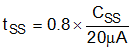
In buck or SEPIC topologies, the soft-start time (tSS) is calculated in Equation 8.
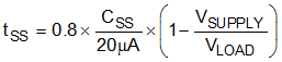
In boost topology, tSS varies with the input supply voltage because the boost output voltage is equal to the boost input voltage at the beginning of the soft-start switching. tSS in boost topology is calculated in Equation 9.
In general, it is recommended to choose a soft-start time long enough so that the converter can start up without going into an overcurrent state.
The device also features an internal 80-mV FB-to-SS clamp which is enabled after eight cycles with current limit. This clamp helps to minimize start-up surges after output shorts or overload situations.